Resist Materials and Nanolithography
- PDF / 4,798,960 Bytes
- 12 Pages / 417.6 x 639 pts Page_size
- 60 Downloads / 302 Views
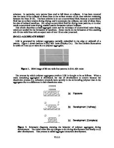
ABSTRACT The work focuses on lithographic processes and materials for sub-50 nm lithography. Lithographic results of polymethyl methacrylates of molecular weights of 50,000, 100,000), 496,000, and 950, 000 are compared. It was found that the molecular weight and developer concentration do not affect smallest linewidth, within experimental error. However, the molecular weight does affect the line-to-line resolution in dense gratings of 40-60 nm in contrast and developer induced swelling. 40 nm period gratings are shown. The work next examines the use of chemically amplified resists for nanofabrication, with a focus on SAL-601. Sub-50 nm lines are defined with latitude of an order of magnitude in dose and a factor of two in post exposure bake time. The results are modeled with a diffusion reaction kinetic model and an approach to optimize resolution and reproducibility is presented. Challenges to attaining the ultimate resolution and line-to-line resolution in polymeric resists include contrast, mechanical stability, swelling, and adhesion. Metal binding self assembled monolayers (SAMs) are presented a class of resists, that circumvent the latter three complications. Work at the Naval Research Laboratory on SAM resists is outlined. INTRODUCTION Nanolithography was reported as early as 1964, when Broers' defined 50 nm lines by ebeam writing a contamination pattern. By the late 1960's, the development of polymethyl methacrylate (PMMA) as an e-beam resist was well in progress.2 PMMA has been the standard high resolution resist for over 30 years. Several reports have cited linewidths defined in PMMA of 10-20 nm in the laboratory.34 Over this time period, the microelectronics industry has progressed at a phenomenal pace and sub-100 nm device dimensions are projected in manufacturing in the next decade. 5 Manufacturing applications present many new challenges to nanolithography including throughput and tight critical dimension control. E-beam resist sensitivities critical dimension (CD) error budgets, specified on the SIA 1997 Roadmap5, are - 110 PtC/cm 2 and 5-10%k, respcetively. The error budgets of 5-10 nm or less, presents a real challenge for polymeric and the multi-component chemically amplified resists. Due to scattering processes during lithographic exposure, higher resolution lithography frequently requires increasingly thinner resists. This in turn, puts increasing demands on etch resistance of the resists. In this work, the nanolithographic performance of resists is examined through electron beam and scanning tunneling microscope exposures. These techniques provide the very high resolution to enable study of the materials properties of the resists. The work begins with an examination of the effects of the macromolecular properties of PMMA on its ultimate resolution. Next the high sensitivity, multi-component chemically amplified resists (CARs) are addressed through an in-depth study of SAL-601. The paper ends with a description of novel resists, developed at the Naval Research Laboratory based upon metal binding
Data Loading...