Electrochemical Dip-pen Nanolithography of Conductive Wires
- PDF / 472,661 Bytes
- 6 Pages / 595 x 842 pts (A4) Page_size
- 28 Downloads / 419 Views
0901-Ra05-09-Rb05-09.1
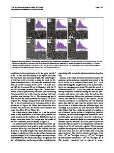
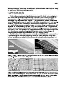
Electrochemical Dip-pen Nanolithography of Conductive Wires Fapei Zhang1, Ryo Yamada1,2 and Hirokazu Tada1,2 1 Division of Materials Physics, School of Engineering Science, Osaka University, Japan 2 JST-CREST ABSTRACT We have explored the fabrication of conductive nanowires on different types of substrates by electrochemistry-assisted DPN (E-DPN) with an atomic force microscope. Various parameters of E-DPN were examined systematically including the effects of coating methods and the types of the tips on the electrodeposition behavior. It was found that a chemically-modified Si AFM tip is very suitable for E-DPN. Platinum and polyaniline nanowires with a line width of ca.100 nm to sub- 100 nm were prepared on the metallic (Au) and semiconducting (Si) surfaces. The parameters indispensable for E-DPN of metal and polymer nanowires on an insulating SiO2 surface are also discussed. INTRODUCTION Fabrication of nanostructures (wires and dots etc) with precise location is a key technology in nanoelectronics and molecular electronics. The conductive nanowires with such a feature can act as nanoelectrodes to interconnect with quantum dots and molecules to prepare nano-devices. This makes it possible to directly wire up the pre-selected molecules in a controlled manner to overcome the large irreproducibility of device fabrication and interconnection problem occurring on the nano-gap contacts produced via normal techniques including break-junction and electroplating. Recently dip-pen nanolithography (DPN) has been invented, in which an atomic force microscope (AFM) tip is used as a “nib” to deliver the molecules onto the substrate via tiny water meniscus at the tip-substrate interface [1, 2]. Various organic and inorganic nanostructures have been written directly on the suitable surface with a high degree of control over location and geometry [3-5]. Such a technique has also been extended for material deposition via electrochemical reaction, which is called electrochemical DPN (E-DPN), since the meniscus can act as a nanometer-sized electrochemical cell. Some different kinds of metal nanowires have been fabricated on Si-base substrates by Li et al [6, 7]. However, E-DPN is a delicate dynamic process, and it depends strongly on various factors of the deposition condition, including humidity, bias applied as well as type and scan rate of the AFM tip. These E-DPN parameters also vary with different type and structure of the substrate. Up to now the effects of these factors on the E-DPN process is still poorly understood. In this study, we have examined the parameters for E-DPN of conductive nanowires on metallic and semiconducting surfaces. In addition, since the deposition of conductive nanowires on an insulating surface (e.g. SiO2) should be more favorable in the fabrication of electronics devices, we also explore the fabrication of such nanowires on an insulating SiO2 surface by E-DPN. EXPERIMENT Two kinds of substrates were examined for E-DPN. One was a p-type Si (111) wafer (5-10
0901-Ra05-09-Rb05-09
Data Loading...