Scanning tunneling microscope observations of polymer fracture surfaces
- PDF / 2,102,490 Bytes
- 11 Pages / 576 x 792 pts Page_size
- 14 Downloads / 323 Views
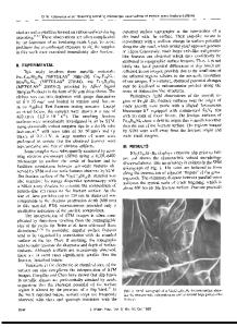
Scanning tunneling microscope observations of gold-coated polymer fracture surfaces are reported. We compare nm-scale surface features of poly(methyl methacrylate) (PMMA) fractured under three different loading conditions: in tension at room temperature, in tension at liquid nitrogen temperature, and in the double torsion geometry at room temperature (slow crack growth). Fracture surfaces of polystyrene and polycarbonate loaded in tension at room temperature are also described. Each of these surfaces shows distinctive nm-scale features which we interpret in terms of the interaction between craze growth (fibril formation) and crack growth along the craze boundary. The resolution of these images is sufficient to greatly complement other fractographic studies.
I. INTRODUCTION Observations of fracture surface topography (fractography) have contributed greatly to our understanding of fracture,1 since many important fracture processes are reflected in surface features. In the case of brittle fracture, fractography is especially valuable because direct observation of the very rapid crack growth in brittle materials is quite difficult. The development of scanning tunneling microscopy (STM) offers the possibility of resolving the topography of smooth conducting and semiconducting surfaces to atomic levels. Atomic force microscopy (AFM) has provided similar information on smooth insulating surfaces, e.g., NaCl (Ref. 2) and BN.3 Atomic resolution has not been achieved with either technique on rougher surfaces, which are commonly encountered in brittle fracture. Nevertheless, the subnanometer resolution of AFM and STM on fracture surfaces is in many instances a substantial improvement over alternate microscopies. Although insulators lack the necessary conductivity for direct STM observations, these materials can be imaged with somewhat reduced resolution after applying thin (10-60 A) films of a conducting material.4"6 We estimate the horizontal resolution of our method applied to polymer surfaces to be on the order of 0.5 nm. Since relatively rough surfaces cannot now be imaged with atomic resolution, the lack of atomic resolution with coated surfaces is not a serious limitation relative to the principal alternative, AFM. However, in any probe-based microscopy, images of rough surfaces can be distorted due to the nonnegligible size of the probe tip relative to the size of the imaged features. Reiss et al? and Denley have addressed this problem for the case of the STM.8 In most cases, artifacts due to surface-tip interactions are readily identified. Although the fracture surfaces 1292 http://journals.cambridge.org
J. Mater. Res., Vol. 7, No. 5, May 1992 Downloaded: 18 Mar 2015
discussed below may be considered rough on the nmscale, we emphasize that they are all microscopically quite smooth. Regions with vertical relief greater than a few hundred nm cannot be reliably imaged with our instrument. In this work we describe STM observations of goldcoated polymer surfaces formed under a variety of conditions. These include fractu
Data Loading...