Sb 2 S 3 /SnSe thin film solar cells by thermal evaporation
- PDF / 9,445,301 Bytes
- 6 Pages / 612 x 792 pts (letter) Page_size
- 9 Downloads / 432 Views
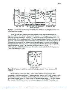
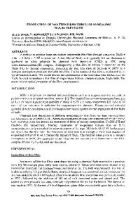
Sb2S3/SnSe thin film solar cells by thermal evaporation José Escorcia-García, Enue Barrios-Salgado, M.T.S. Nair, and P.K. Nair Instituto de Energías Renovables – UNAM, Priv. Xochicalco S/N, Temixco, Morelos 62580, México. ABSTRACT We report a stable CdS/Sb2S3/SnSe heterojunction thin film solar cell deposited on SnO2:F (FTO) – coated glass substrates. Thermal evaporation at 10-5 Torr with substrate temperature of 400 °C was used to deposit Sb2S3 and SnSe thin films of 450 nm and 160 nm, respectively. Thin film Sb2S3 has an optical band gap (Eg) of 1.48 eV and photoconductivity (σp) of 4x10⁻⁷ Ω-1 cm-1 and thin film SnSe has an Eg of 1.28 eV and σp of 2 Ω-1 cm-1. The chemically deposited CdS thin film heated at 400 °C shows an Eg of 2.34 eV and σp of 0.1 Ω-1 cm-1. Stabilized solar cell structures with these thin films, FTO/CdS/Sb2S3/SnSe/C-Ag, showed open circuit voltage (Voc) of 0.60 V, short circuit current density (Jsc) of 5.51 mA/cm2 and power conversion efficiency (η) of 0.96% with a fill factor FF of 0.29. In the absence of the SnSe layer, Jsc decreases to 4.77 mA/cm2. INTRODUCTION Thin films of Sb2S3 having optical absorption coefficient (α) > 105 cm-1 in the visible region and Eg of 1.88 eV have been integrated in different types of solar cells [1-4]. In all these solar cells Sb2S3 requires a thermal treatment above 240 °C to improve the crystallinity and thus, photovoltaic parameters. Since the electrical conductivity of Sb2S3 is around 10-7-10-6 Ω-1 cm-1, the internal electric field Eint, induced across the Sb2S3 layer is weak, resulting in excessive recombination loss in the Sb2S3 layer. Thus, an optimum film thickness is also required to improve the performance of the Sb2S3-based solar cells [5]. Different authors have proposed the use of a p-type material or hole transporter to enhance the Eint across the Sb2S3 [3, 6]. SnSe is a ptype semiconductor with orthorhombic crystal structure and has both an indirect (0.9 eV) and a direct (1.30 eV) band gap with α of 105 cm-1 in the visible region [7]. Thin film and nanocrystal SnSe absorbers are reported in solar cells [8-10], in which this material has been deposited by different techniques such as solution phase synthesis [8] and electrodeposition [9,10]. The best result has been obtained for the solid state device, ITO-CdS-SnSe-Au [10], which shows an open circuit voltage Voc of 0.37 V, a short circuit current density Jsc of 5.37 mA/cm2, and power conversion efficiency η of 0.8%. By using a polysulfide electrolyte in a liquid junction device, ITO-CdS-SnSe-polysulfide-Pt-FTO, the efficiency improved to 1.4% due to enhanced carrier transport through the polysulfide electrolyte. In the present work we have used SnSe thin film as a p-type material in the FTO/CdS/Sb2S3/SnSe/C-Ag structure in order to improve the internal electric field across the Sb2S3 layer and thus the solar cell performance. EXPERIMENTAL DETAILS The SnO2:F (FTO) - coated glass substrates having a sheet resistance of 15 Ω were washed with neutral soap and water followed by cleaning with ultrasoni
Data Loading...