Selection Rules in the Raman Spectrum of Porous Silicon
- PDF / 258,653 Bytes
- 5 Pages / 412.92 x 646.2 pts Page_size
- 70 Downloads / 338 Views
571
Mat. Res. Soc. Symp. Proc. Vol. 452 01997 Materials Research Society
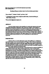
EXPERIMENT Porous silicon films were prepared on (001) boron doped p-type silicon wafers (0.1-0.5 Q.cm). Samples were etched in a 2:1 solution of HF and ethanol. Different current densities and formation times were used. Etching was done either under illumination or in the dark. Only samples etched under illumination showed strong photoluminescence. Raman spectra were measured with a Renishaw Ramascope spectrometer. Light from an argon laser (514.5 nm) or a helium-neon laser (632.8 nm) was focused onto the (001) surface through an optical microscope. The power density was kept smaller than 24 W/cm2 to avoid any heating effects. Light scattered by the sample was collected through the same microscope and analyzed by a grating spectrometer. Elastically scattered light was rejected by a supernotch holographic filter. Polarization directions were along the crystallographic axes. RESULTS Figure 1 depicts the Raman spectra measured in two samples etched for 1 minute under different conditions. One was etched in the dark (spectra on left column) and the other was etched under illumination (spectra on right column). Spectra on the upper and lower rows were
Etched in the dark
Etched under illumination
-Z(XY)Z U
Z(XX)Z
632.8 nm
x1 2 An
'
I
I
'
UgW
U...U --- , U ,
500
510
t ,
520
514.5 nm
,m
530
510
Raman shift
(cm"1)
520
530
Fig. 1. Raman spectra measured for two porous silicon samples etched for I min at 6 mA in the dark (left column) and under illumination (right column). Upper and lower row spectra were excited, respectively, at 632.8 and 514.5 nm. Full lines stand for the allowed configuration and dots to the forbidden configuration. Latter spectra were multiplied by the indicated factor.
572
excited with light of 632.8 and 514.5 nm, respectively. The phonon peak is always wider for the shortest wavelengths, as has been previously observed [7]. This has been attributed to the larger penetration depth at longer wavelengths, together with a smaller pore size in the deeper layers [7], or to a resonance effect [8]. The most striking result is that for the sample etched under illumination the Raman peak is mostly depolarized, with no change in lineshape from one polarization to the other. However, for the sample etched in the dark, the peak in the forbidden configuration is one order of magnitude smaller and much broader than for the allowed configuration. Samples etched in the dark are always more homogeneous when observed under an optical microscope. Therefore we think that in the samples formed with light microscopic roughness produces a great deal of scattering and a strong depolarization of light. In the forbidden configuration one observes the peak corresponding to the allowed configuration, which is the LO phonon broadened by quantum confinement. The porous silicon film is only a few microns thick. Since the light penetration depth is of the same order of magnitude, the peak in the allowed configuration could have som
Data Loading...