Selective Area Growth of GaN Nano Islands by Metal Organic Chemical Vapor Deposition: Experiments and Computer Simulatio
- PDF / 451,990 Bytes
- 6 Pages / 612 x 792 pts (letter) Page_size
- 49 Downloads / 292 Views
0955-I07-14
Selective Area Growth of GaN Nano Islands by Metal Organic Chemical Vapor Deposition: Experiments and Computer Simulations Anilkumar Chandolu1, Gela D Kipshidze1, Sergey A Nikishin1, Lu Tian2, Song Daoying2, Mark Holtz2, and Anya Lobanova3 1 Department Of Electrical and computer Engineering, Texas Tech University, 1012 Boston Avenue, Mail Stop 3102, Lubbock, TX, 79409-3102 2 Department of Physics, Texas Tech University, Campus Box 41051, Lubbock, TX, 79409-1051 3 Soft-Impact, Ltd., P.O. Box 33, St.-Petersburg, 194156, Russian Federation
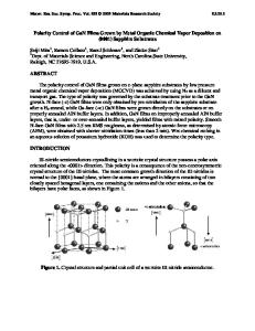
ABSTRACT We report the properties of GaN islands selectively grown by MOCVD on (0001) GaN/sapphire templates and on bare (0001) sapphire substrates. The approach allows us to grow GaN crystals with control over size and density through optical (micro-scale) and scanning electron microscope (SEM) e-beam (nano-scale) lithography. We have obtained complete pyramidal and prismatic hexagonal GaN islands. The growth characteristics are found to be very different from what we obtain for epitaxial layers, an effect which is attributed to loading and surface diffusion of source materials on the hard mask. From the dependence of growth rate of the pyramids with pitch we evaluate Ga surface diffusion length of ~ 10 µm over SiO2 mask. We present a growth model based on diffusion and compare the results of modeling with our data. Using micro-Raman spectroscopy the stress in pyramidal and prismatic islands was evaluated to be 50 ± 17 MPa and 84 ± 20 MPa, respectively. This implies that the islands are nearly relaxed compared to similar thickness of uniform layers. Room temperature SEM cathodoluminescence (CL) shows a narrow linewidth consistent with high quality of GaN layers. The GaN islands, of varying shapes, were overgrown with InGaN multiple quantum wells, with optical properties measured using SEM-CL. INTRODUCTION Recent interest in growth of nanostructures has focused on two approaches, vapor-liquidsolid (VLS) epitaxy and selective area growth (SAG). VLS growth has demonstrated high quality GaN [1-6] and AlGaN wires [7, 8]. The VLS process utilizes a molten metal catalyst on a substrate with limited control over uniformity in length, diameter, shape, and position to produce isolated nanostructures, along with any effects of VLS metal contamination. The SAG of GaN is carried out via metalorganic chemical vapor deposition (MOCVD) without the use of a catalyst. It is widely established at the micron and up scale [9-12], with fewer reports of submicron SAG of GaN, InGaN, and AlGaN [13-16]. A hard mask such as SiO2 is usually produced on the substrate permitting selective growth in patterned openings (windows) and excluding growth on the mask. In this paper we report the growth of GaN islands using SAG on patterned GaN and sapphire templates by MOCVD. The growth rates of selectively grown islands have been investigated based on the fill factor of SiO2 mask. Simulations have been carried out to address the various diffusion mechanisms and to evaluate the relevant parameters. Multipl
Data Loading...