Self Assembled Monolayer Methods in the Fabrication of High-Tc Superconductor SNS Junction Nano-Devices
- PDF / 1,537,946 Bytes
- 6 Pages / 612 x 792 pts (letter) Page_size
- 69 Downloads / 419 Views
J7.4.1
Self Assembled Monolayer methods in the fabrication of High-Tc Superconductor SNS Junction Nano-Devices Sungwook Kim, In Soon Chang, Fannyben Patel, and John T. McDevitt* Department of Chemistry and Biochemistry, Center for Nano- and Molecular Science and Technology, The University of Texas at Austin, Austin, Texas 78712-1167
ABSTRACT Although the superconductor/normal metal (SN) interface is one of the most important controlling factors in determining the performance of superconductor/normal metal/superconductor (SNS) junctions, controlling the SN interface still remains difficult. The in situ deposit techniques have been widely used to cope with this problem, but they limit the types of SNS junctions that can be explored. Soft Chemistry Etching methods were developed to fabricate the YBCO/Au/YBCO and TX-YBCO/Au/TX-YBCO SNS junction nano-devices with ex situ deposit. The planar SNS junctions controlled by such methods exhibited good transport properties above 80 K with less than 10-8 Ω-cm2 contact resistivity. The current state of the suitable fabrication methods of SNS nano-devices will be described with experiment results. INTRODUCTION The superconductor-normal metal-superconductor (SNS) junction has been a promising configuration for applications such as sensors, electronics, and possible quantum computers.1, 2 Although the SN interface is the most important controlling factor in determining the performance of SNS junctions, controlling the superconductor/normal metal (SN) interface still remains difficult. The difficulty comes from several aspects of the materials and fabrication methods such as lattice mismatch and chemical incompatibility between superconductors and normal metals.3 However, the major stumbling block to control the interface problems could be degradation of the superconductor material itself. Soft chemistry approaches for High-Tc superconductor (HTSC) surface modifications are particularly important for the practical fabrication of superconducting electronic material devices as well as to explore the different types of SNS junctions. We have demonstrated previously different types of soft chemistry for superconductor surface modification, such as corrosion passivation, 4 polymer growth, 5, 6 coordination chemistry, 7 and surface cleaning.8 Herein, we report an expanded study of the surface and nano-trench cleaning of HTSC devices. Self assembled monolayer (SAM) can be used as an etching method for the surface and nano-trench of cuprate superconductor devices as shown by AFM study, four-point measurement, and scanning electron microscopy (SEM) study.
J7.4.2
ex-situ deposit: 300 nm Gold
S
N
S
400 nm
MgO
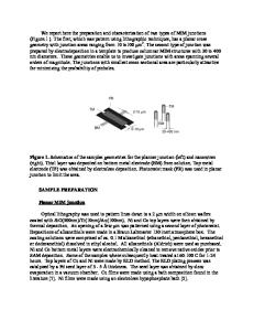
40 – 60 nm
Figure 1. Schematic illustration of High-Tc superconductor SNS nano-device dimension. EXPERIMENTAL DETAILS High quality YBa2Cu3O7-δ (YBCO) and Y0.6Ca0.4Ba1.6La0.4Cu3O7-δ (TX-YBCO) thin films were deposited by standard ablation methods on (100) MgO single crystal substrates. The typical thickness of the films was 4000 Å for both samples. The c-axis oriented films exhi
Data Loading...