Electroless Cu Deposition on Self-assembled Monolayer Alternative Barriers
- PDF / 971,706 Bytes
- 7 Pages / 612 x 792 pts (letter) Page_size
- 76 Downloads / 320 Views
1156-D04-08
Electroless Cu Deposition on Self-assembled Monolayer Alternative Barriers S. Arminia, A. Maestre Caroa,b a b
IMEC, Kapeldreef 75, B-3001 Heverlee, Leuven, Belgium Katholieke Universiteit Leuven, Kasteelpark Arenberg 1, B-3001 Heverlee, Belgium
* corresponding author: Silvia Armini, IMEC, Kapeldreef 75, B-3001 Leuven, Belgium. Tel.: +32 (0) 16 28 86 17. Fax. : +32 (0) 16 28 13 15. E-mail: [email protected]
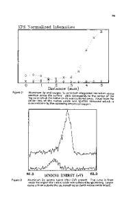
ABSTRACT An alternative bottom-up Cu electro-less deposition (ELD) method without other catalyst material activation tested on blanket wafers, is the focus of this paper. The process consists in reducing the Cu ions via standard reducing agents, such as dimethylamine borane (DMAB). A wide range of experimental conditions such as pH, temperature, Cu ion concentration and time are investigated and the Cu layer nucleation and growth mechanism is evaluated on clean SiO2 and after functionalization with 3aminopropyltrimethoxysilane (APTS) self-assembled monolayer (SAM) used as copper diffusion barrier. The barrier properties of the APTS layer after Cu ELD are also assessed by copper resistivity measurements and visual inspections as a function of the annealing temperature. INTRODUCTION Due to the several applications of metalized organic layers in organic/molecular electronics [1], polymer light emitting diodes [2], food packaging and prosthetic implants [3], there is an increasing interest in understanding and controlling the interaction between metals and organic films [4, 5, 6, 7] Cu is the interconnect material of choice in the metallization step for advanced semiconductor device manufacturing. A typical interconnect structure is composed of Cu/Ta/TaN/SiO2 where the Ta/TaN layer is required as a barrier to prevent interdiffusion between Cu and the underlying dielectric resulting in electrical shorting. Due to its poor electrical conductivity, relative to Cu, the barrier layer thickness must be minimized while maintaining high performance diffusion barrier properties and good adhesion strength with neighboring layers. Nevertheless, barrier layer formation has become increasingly difficult as the technology node is reduced. An alternative to the conventional barrier process is an organic “selfassembling” system, so-called self-assembled monolayer (SAM). This inherently bottom-up process involves the anchoring of bi-functionalized organic molecules on the inter-layer dielectric (ILD) surface. There are many potential advantages of SAMs vs. metal-based barriers: i) conformality, ii) coverage in high aspect ratio (HAR) structures, iii) selectivity, iv) tailored surface functionalization to control reactivity, v) modulation of line resistance. The current approaches to Cu metallization include chemical vapor deposition (CVD), physical vapor deposition (PVD), selective electroless deposition (ELD) and electroplating. As device sizes decrease, accommodated by scaling and materials changes, electrochemical deposition is considered the most promising method due to its many advantages such as good uniformi
Data Loading...