Silicides for Infrared Applications
- PDF / 1,387,956 Bytes
- 9 Pages / 414.72 x 648 pts Page_size
- 58 Downloads / 404 Views
PAUL W. PELLEGRINI, Rome Laboratory, Electromagnetic Devices Technology Division, Hanscom AFB, MA 01731-2909
ABSTRACT This paper discusses the attributes of metal silicides as they are applied to detection of infrared photons. These materials have a long history in the silicon community as interconnects and are easily integrated into manufacturing. The technology is currently only sensitive to 10 pm in the infrared. New results obtained from silicon germanium alloys are discussed that will help overcome these spectral limitations. INTRODUCTION The use of metal based silicides on substrates of silicon for detection of infrared radiation is a relatively new technology. The original idea for using two dimensional arrays of these detectors to perform staring sensing was proposed in 1973 by Shepherd and Yang'. These detectors work by internal photoemission. Previously, infrared detectors were made from compound semiconductors using intrinsic detection. The first successful system use of infrared detectors was in 1950's, where lead salts were used by the military for heat seeking missiles. Advances in both the US and UK in narrow bandgap, compound semiconductors led to the development of direct bandgap materials for infrared detection. The most widely known of these direct gap semiconductors are HgCdTe and InSb. In the past 40 years, the military has invested heavily in these intrinsic detector technologies. However, the fact that those material systems use a substrate that is not the industry standard of silicon, means that they cannot be made into
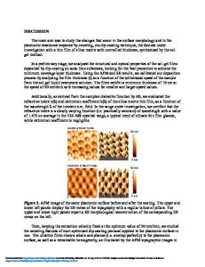
large two dimensional arrays and they are expensive to produce. The most successful photoemissive infrared detector material to date is platinum silicide (PtSi) deposited on high quality, VLSI grade silicon. This material system has been studied extensively by researchers because of its use as a high reliability interconnect and ohmic contact material for the silicon industry. Its cost is higher than that of other more standard materials like aluminum, and its refractory nature demands that it be deposited using electron beam (e-beam) melting in Ultra High Vacuum (UHV) chambers. Its ability to carry large currents over long periods of time without electro migration has led companies with leased electronics to use it extensively. It is less expensive to make high reliability contacts, than to replace circuit boards in the field with failed contacts. PtSi has advanced rapidly since its discovery, and infrared cameras have been developed which operate at standard television display rates, using f/2 optics, that can distinguish temperature differences of less than 0.01*C. These arrays have more than 300,000 individual detectors in a 480(V)x640(H) format. They include a readout made from Charge Coupled Devices (CCD's) or from switched CMOS FET's. A monolithic structure having both detectors and readout on the same integrated circuit is important for reliability and cost considerations, but infrared optical performance suffers because of the silicon area that must be devoted to s
Data Loading...