Size-controlled deposition of Ag and Si nanoparticle structures with gas-aggregated sputtering
- PDF / 8,801,089 Bytes
- 7 Pages / 612 x 792 pts (letter) Page_size
- 28 Downloads / 259 Views
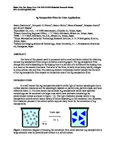
Size-controlled deposition of Ag and Si nanoparticle structures with gas-aggregated sputtering Cathal Cassidy, Vidyadhar Singh, Zafer Hawash, Murtaza Bohra, Jeong-Hwan Kim, Mukhles Sowwan Okinawa Institute of Science and Technology (OIST), 1919-1 Tancha, Onna-son, 904-0495, Japan ABSTRACT Physical vapor deposition, in combination with gas-aggregation (PVD-GA), is a controllable method for creation of diverse nanoparticle structures. Given the size effects that dominate the physics of nanoparticles, a particular advantage of the PVD-GA technique is the compatibility with in situ mass filtering of the nanocluster beam. In the current work, PVD-GA has been utilized to deposit Ag and Si nanoparticles. Nanoparticles were analyzed using in situ quadrupole mass spectrometry (charge/mass ratio), atomic force microscopy (nanoparticle height), and transmission electron microscopy (nanocluster diameter & crystallinity). The results for particle size distribution were crosscorrelated, with excellent agreement. Different growth methods & conditions were explored, resulting in controlled differences in the measured particle size distributions and surface coverage. A novel growth configuration utilizing a conventional sputter source in combination with a linear magnetron allowed a significant (fivefold) increase in Ag cluster yield. INTRODUCTION It is well known that materials in nanoparticle form may exhibit properties quite different to the corresponding bulk materials. The enhanced properties, and exciting applications that may be explored are related to the nanoscale size constraints, enhanced surface area, and possible entry into biological cells. In particular, the size effect is very attractive for technological application, in that it offers the possibility to engineer optical, magnetic or electrical properties simply by changing the nanoparticle size. In the current work, first characterization data from a newly-installed nanoparticle deposition system, is reported. For this early work, Ag and Si were chosen as characterization materials. These materials have been extensively studied, and are attractive for a range of scientific and technological applications. For example, Ag nanoclusters manifest interesting optical properties, as the plasmon resonance of this metallic material can be tuned by changing the nanoparticle size [1]. Si nanoparticles are an example of semiconductor quantum dots, with a distorted band structure and corresponding differences in optical and electronic properties [2]. EXPERIMENT Nanoparticles were deposited using a gas-aggregated sputtering system from Mantis Deposition Ltd (Oxon, UK). The gas-aggregated sputtering technique was originally reported by Haberland et al. [4]. The interested reader is referred to [5-7] for exemplary recent works. The nanoparticle deposition system is illustrated in Fig. 1. Materials were sputtered using an Ar plasma, from 25mm targets. An initial high-pressure aggregation zone is formed by restricting the pumping of the region via a 5mm aperture, and water-cooling th
Data Loading...