Solid Solubility of Sb and Te Implanted GaAs Following Solid Phase Annealing
- PDF / 273,499 Bytes
- 5 Pages / 420.48 x 639 pts Page_size
- 103 Downloads / 231 Views
SOLID SOLUBILITY OF Sb AND Te IMPLANTED GaAs FOLLOWING SOLID PHASE ANNEALING
S.T. Johnson, K.G. Orrman-Rossiter and J.S.Williams Microelectronics Technology Centre, Royal Melbourne Institute of Technology Melbourne, Australia 3000.
ABSTRACT High dose antimony and tellurium implanted (100) GaAs wafers have been annealed in the solid phase under various time/temperature conditions using a conventional furnace, a rapid incoherent light source and a continuous wave CW Argon ion laser. The samples were capped with RF sputtered Si0 2 prior to annealing and analysed using 2MeV He++ ion channeling to determine the solid solubility of the implanted ions. Results indicate that the Te is more soluble than Sb; highest 3 2 0 for Te and 1.3 x 10²⁰ solubilities measured were 6 x 10 cmcm-3 for Sb.
INTRODUCTION The annealing of ion implanted GaAs is particularly complex in comparison with that of Si. The implantation damage is not usually removed by epitaxial 0 crystallisation (which occurs at < 250 C) and temperatures exceeding about 0 600 C are normally required to anneal out residual crystalline disorder to give good single crystal recovery[1 - 3 . This complicated damage-removal behaviour, together with the necessity to protect the GaAs surface from dissociation during heating at temperatures above 5000C,[1,21 most probably accounts for the paucity of solid solubility data for ion implanted GaAs. In this paper, we outline a method for conveniently measuring solid solubilities of implants in GaAs following furnace heating and more rapid solid phase annealing. The method, which employs ion channeling analysis through a thin Si0 2 cap, has been used to measure the solubility of implanted Te and Sb in (100) GaAs.
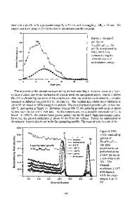
EXPERIMENTAL Single crystal (100) GaAs wafers were implanted at LN 2 temperatures with 90 keV Sb+ and 100 keV Te+ ions to fluences in the range 1 x 10 14 cm- 2 to 6 2 1 x 101 cm- . An encapsulant layer of Si0 2 was RF sputter deposited on front and back sides of the wafers to prevent surface dissociation of GaAs during annealing. The oxide layers deposited on the implanted surface of the wafers were kept below 400R in thickness to allow analysis of the solubility of the implanted species by 2MeV He++ ion channeling, without removal of the encapsulant layer. Fig.l shows typical random and aligned RBS spectra for 5 3 x 101 Sb cm-n implant, followed by deposition of -340 R of Si0 2 . The spectra clearly indicate the signals from the oxygen and silicon in the encapsulant which are superimposed on the signal from the underlying GaAs. The signal from the implant appears at higher energies, allowing the nearsubstitutional Sb fraction to be estimated from the integrated random and aligned yields once the implantation damage has been removed by an annealing step. Implanted, encapsulated samples were annealed by one of three methods: i) furnace heating in a flowing N2 ambient at temperatures of 600 0 C and 8500C, ii) heating for times of 10 and 20 sec using an incoherent light source t41at
Hat. Res. soc.Symp. Proc. Vol. 23 (198
Data Loading...


