Beam Annealing of Ion-Implanted Gaas and Inp
- PDF / 3,341,521 Bytes
- 14 Pages / 415.8 x 637.2 pts Page_size
- 106 Downloads / 431 Views
261
BEAM ANNEALING OF ION-IMPLANTED GaAs AND InP J. C. C. FAN, R. L. CHAPMAN, J. P. DONNELLY, G. W. TURNER, Lincoln Laboratory, Massachusetts Institute of Technology Lexington, Massachusetts 02173
AND C. 0.
BOZLER
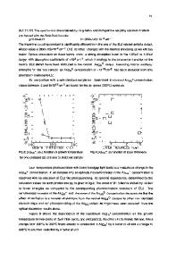
ABSTRACT A scanned cw Nd:YAG laser was used to anneal ionimplanted GaAs and InP wafers. Measurements show that electrical activation is greater for p-type than for n-type dopants in GaAs, while in InP, the opposite is observed. A simple Fermi-level pinning model is presented to explain not only the electrical properties we have measured, but also those observed by other workers. We have fabricated GaAs and InP solar cells with junctions formed by ion implantation followed by laser annealing. The GaAs cells have much better conversion efficiencies than the InP cells, and this difference can be explained in terms of the model. INTRODUCTION Recently, there has been much activity in the electron and laser beam treatment of semiconductors. Much of the work has been on Si and has involved either the crystallization of amorphous Si films [1] or the annealing of ion implanted Si [2]. Far less has been reported on compound semiconductors such as GaAs and InP. This paper briefly reviews the current status of beam annealing of ion-implanted GaAs and InP. We propose a model to explain the results that have been reported by various workers, and then present our results in the context of the model. In particular, detailed measurements on GaAs are presented to illustrate the effects of the defect formation on electrical properties. Finally, we recommend annealing conditions that we believe will provide the best chance of obtaining good activation in these compound semiconductors. The current results of beam annealing of ion-implanted GaAs and InP samples can be classified into two categories-samples with implant dosages at 14 2 or greater than 10 cm- , and samples with implant dosages lower than 2 14 2 10 cm- . GaAs samples with implant dosages around 1 x 10 cmhave reasonably good activation [3,4,5] with beam annealing. However, the Hall mobility values are always lower than those obtained by conventional thermal annealing. The activation becomes even better [6,7,8,9] when implant dosages 15 2 are higher than I x 10 cm- . There is also a consistent trend that p-type dopants activate more easily than n-type dopants at comparable implant dosages. In low-dosage implanted GaAs, beam annealing processes often have produced no activation or very low activation. Only three groups [3,10,11] have reported reasonably good activation on samples with low implanted dosages. All three groups obtained their results with a cw scanning laser or electron beam. Beam annealing of InP samples implanted with high dosages of either Se or Si (n-type) has been reported by three groups [3,12,13]. The electrical activation after annealing was generally good. However, the Hall mobility values are lower than those obtained by conventional thermal annealing. There are no published results on beam annealing of low-dosage implanted n-type InP. No
Data Loading...