Strained SiC: Ge Layers in 4H SiC formed by Ge Implantation
- PDF / 87,800 Bytes
- 6 Pages / 612 x 792 pts (letter) Page_size
- 34 Downloads / 325 Views
K6.7.1
Strained SiC:Ge Layers in 4H SiC formed by Ge Implantation M.W. Dashiell, G. Xuan, Xin Zhang, E. Ansorge and J. Kolodzey Department of Electrical and Computer Engineering University of Delaware Newark, DE 19716
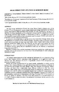
ABSTRACT The ion implantation of germanium into 4H-SiC at 1000 oC resulted in crystalline SiC:Ge layers that are coherently strained to the (0001) oriented 4H-SiC substrates. Germanium implantation energies of 140 keV and 50 keV were chosen to form approximately 100nm thick step-like SiC:Ge layers with Ge atomic fractions ranging from 0.0007 to 0.006. High-resolution x-ray diffraction (HRXRD) and reciprocal space mapping reveal a high-quality, compressively strained SiC:Ge layer. High-temperature annealing resulted in partial relaxation of the macroscopic layer strain, however the SiC:Ge layer remained strained with a coherent interface for annealing up to at least 1650oC. Because Ge is a group-IV atom like Si and C, its incorporation into the lattice is expected to act as an isoelectronic impurity, rather than a charged donor or acceptor. Thus, high-quality, SiC:Ge layers have the potential for bandgap and strain engineered electronics such as SiC-based high electron mobility transistors (HEMTs) for RF-power electronics. Currently there is no established heterojunction pair in SiC material technology for fabricating HEMTs and other heterojunction devices.
INTRODUCTION Silicon carbide is an important wide bandgap semiconductor whose intrinsic properties make it suitable for high-temperature and high-power microwave devices [1-2]. Unlike III-V wide bandgap materials however, the lack of a well developed SiC-based heterostructure system limits the ultimate performance of SiC devices compared to nitride based high bandgap devices such as the AlGaN/GaN high-electron-mobility-transistor (HEMT). Recently there have been a number of investigations of the material and structural characteristics of semiconductor SiC after implanting Ge ions into the SiC crystal. Depending on the implantation and post-implant conditions, the resulting layer may exhibit one or more of the following: (1) amorphization due to heavy radiation damage, (2) re-crystallization into one of several different SiC polytypes, or (3) phase separation of Ge nanocrystals embedded within the SiC lattice [3-4]. There has been little experimental work to date however on the use of Ge ion-implantation to form a dilute substitutional SiC:Ge alloy as discussed in [5]. Although the group IV elements such as Ge are immiscible in crystalline SiC under equilibrium conditions, the addition of a few atomic percent Ge to form a metastable alloy would offer additional flexibility for high-bandgap SiC electronics by introducing a new group IV material for enabling heterostructure concepts. In this paper we present high-resolution x-ray diffraction measurements of pseudomorphic SiC:Ge layers synthesized on the technologically relevant 4H-SiC substrate.
K6.7.2
Dilute Ge contents (on the order of 1 percent) were chosen so that layer strains were not so lar
Data Loading...