Stress Generation in PECVD Silicon Nitride Thin Films for Microelectronics Applications
- PDF / 119,757 Bytes
- 6 Pages / 612 x 792 pts (letter) Page_size
- 31 Downloads / 367 Views
B7.9.1/O11.9.1
Stress Generation in PECVD Silicon Nitride Thin Films for Microelectronics Applications M. Belyansky, N. Klymko, A. Madan, A. Mallikarjunan, Y. Li, A. Chakravarti, S. Deshpande, A. Domenicucci, S. Bedell, E. Adams, J. Coffin, L. Tai, S-P. Sun1 , J. Widodo2 and C-W Lai2 IBM Semiconductor R&D Center, Hopewell Junction, NY 12533, USA 1 Advanced Micro Devices, Inc; Hopewell Junction, NY 12533, USA 2 Chartered Semiconductor Manufacturing; Hopewell Junction, NY 12533, USA
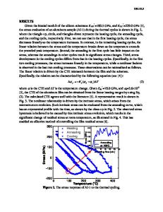
ABSTRACT Thin SiN films deposited by plasma enhanced chemical vapor deposition (PECVD) have been analyzed by a variety of analytical techniques including Fourier Transform Infrared Spectroscopy (FTIR), X-ray reflectivity (XRR), and Rutherford Backscattering Spectrometry/Hydrogen Forward Scattering (RBS/HFS) to collect data on bonding, density and chemical composition respectively. Both tensile and compressive SiN films have been deposited and analyzed. Mechanisms of stress formation in SiN thin films are discussed. It has been found that amount of bonded hydrogen as detected by FTIR is higher for compressive films compared to tensile SiN films. Amount of bonded hydrogen in a film is correlated well with tensile stress. Effect of deposition temperature and other process parameters on stress have been studied. Exposure of SiN films to elevated temperature after deposition lead to increase in tension and degradation in compressive stress. New approaches to stress generation in thin films like creation of multilayer film structures have been delineated.
INTRODUCTION Strain generation in silicon is becoming one of the major knobs in boosting performance of the leading edge metal-oxide-semiconductor field effect transistor (MOSFET) technology [1]. Tensile strain in the silicon channel is beneficial for electron mobility, while compressive stress increases hole mobility. While the basic physics behind stress induced mobility enhancement has been known for many years [2], only recently has stress engineering been incorporated into state of the art microprocessor logic technology. Strain in the silicon channel can be achieved by various techniques. For example, biaxial strain could be applied by depositing silicon on relaxed SiGe substrate, which is beneficial for both electron and hole mobility [3]. However, due to substantial technological difficulties biaxial strain has not been implemented yet in any logic technology. Another way of creating compressive strain in the silicon channel is introduction of an embedded SiGe layer close to the channel. The embedded SiGe approach has been successfully implemented [1], however it is technologically complex and is limited to hole mobility enhancement only. This work explores ways of increasing the intrinsic stress level (both tensile and compressive) in the PECVD Silicon Nitride (SiN) films using various analytical techniques. Substantial increase in device speed has been achieved by application of these highly stressed SiN films, which in turn has been successfully incorporated into dual stress liner
Data Loading...