Stress Stability of PECVD Silicon Nitride Films During Device Fabrication
- PDF / 265,243 Bytes
- 6 Pages / 612 x 792 pts (letter) Page_size
- 14 Downloads / 537 Views
E6.3.1
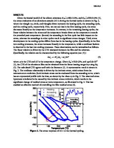
Stress Stability of PECVD Silicon Nitride Films During Device Fabrication Michael P. Hughey and Robert F. Cook Department of Chemical Engineering and Materials Science University of Minnesota, Minneapolis, MN 55455 ABSTRACT Conventional, dense dielectrics serve as structural elements in Cu/low-k interconnect structures, and a full understanding of their thermo-mechanical properties is desired to help optimize device fabrication and avoid mechanical failure. Wafer curvature measurements were made on plasma-enhanced chemical vapor deposited (PECVD) silicon nitride films during thermal cycling to explore the large, irreversible, tensile stress developed. Spectroscopic techniques were used to probe the composition and structure of the films after annealing steps and indicate that reaction of hydrogen-containing defects provides the mechanism for stress change. A simple kinetic model, modified by the inclusion of an equilibrium function of hydrogen defects, is proposed and is found to adequately describe stress development. INTRODUCTION Conventional PECVD films are essentially the only structural elements in Cu/low-k microelectronic interconnect structures. The less dense low-k materials have small modulus, hardness, and toughness and require thin PECVD stop layers to prevent mechanical failure during the critical chemical-mechanical polish processes. Fabrication of a device requires many thermal cycles for the curing or deposition of the low-k and PECVD dielectric material in each layer. Thus, full understanding of a PECVD dielectric’s thermo-mechanical properties is required to help choose materials and processing steps that will reduce mechanical failure of the device, as stress development may be unavoidable. Much effort has been made to measure and model the development of reversible stress caused by thermal expansion mismatches between interconnect materials and the silicon substrate. However, it is well known that PECVD dielectrics contain large amounts of incorporated hydrogen that evolves from the solid film on annealing at, or above, the deposition temperature, causing a change in film structure and the irreversible development of tensile stress. For various PECVD chemistries, this behavior has been attributed to strained bonds resulting from network reformation [1], the diffusion of unbonded molecular hydrogen [2], densification [3], and void annihilation [4]. It is desirable to develop a model to predict stress change for arbitrary thermal histories. Progress is made toward this goal by treating multiple films to different thermal cycles and annealing steps to gain understanding of the effects of temperature and thermal history on the stress change kinetics. EXPERIMENT PECVD silicon nitride (SiNx:Hy) films were deposited using conditions to generate Si-rich films: gas flow rates of 140 sccm SiH4 (2% in He), 1.4 sccm NH3, 520 sccm N2, 900 mTorr total pressure, and 13.56 MHz r.f. power at 34 mW/cm2. Multiple films were deposited at substrate temperatures 150 °C, 250 °C, and 300 °C. Films for stress and
Data Loading...