Strong Blue and Violet Light Emission from Silicon- and Germanium-Implanted Silicon-Dioxide Films
- PDF / 988,408 Bytes
- 6 Pages / 414.72 x 648 pts Page_size
- 75 Downloads / 380 Views
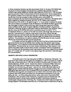
lanted at an energy of 200 keV followed by a second Si' implant at 100 keV using the same doses and substrate temperatures as in the case of Ge÷. As calculated by TRIM, under these conditions a broad implant profile of an average density of excess Si or Ge atoms of about 3 at. % would be achieved over a depth region of 100 to 400 nm below the oxide surface. Postimplantation heat treatment was performed in the temperature range of 400'C to 1200'C for either 30 or 60 min in an N 2 ambient. MOS dot structures for EL studies were prepared using sputtered 300 nm-thick layers of indium tin oxide (ITO) and Al as front- and rear-side electrodes, respectively. The oxide on the rear side of the wafer was removed before Al metallization. The transmission of ITO is higher than 80 % in the wavelength region of 340 nm to 2 .tm. The dot matrix with a dot diameter of 1 mm was made by photolithographic patterning. Finally, thermal processing at 400'C for 30 min was carried out to improve the ohmic properties of the Al contacts. EL and PL measurements were performed at RT in a Spex Fluoromax spectrometer with an R928 Hamamatsu photomultiplier. HREM analysis of cross-sectional samples was carried out in a Philips CM-300 microscope at 300 kV with a line resolution of 1.4 nm. RESULTS AND DISCUSSION Fig. 1 shows PL spectra from Si'- and Ge'- implanted Si0 2 films at different anneal temperatures T. under 250 nm and 240 nm excitation, respectively. The PL peaks around 485 nm (Fig.la) and 410 nm (Fig.lb) are dominant in the PL signals from the Si0 2 layers after implantation of Si' and Ge' ions. Raising T, to 500'C leads to an increase by a factor of 2.5 and 9 in the intensity of the blue and violet PL signals, respectively, which reach maximum values at this temperature. At T. = 5000C the PL intensity from the Ge'-implanted oxide layers exceeds that from the Si'- implanted ones by a factor of 7, thus becoming visible with the naked eye. Annealing at still higher T. quenches progressively the short-wavelength PL. The increase in T, results also in a shift of the PL peak towards the shorter wavelength. For Si'-implanted Si0 2 the 5000
700 50C
70Si+ 600 -A Lex=250 nm 500 M
0
to 300
Xex240 nm
%
4000
6000C
8
ce 400
b)
Ge* soo0c
a)
O
a
d 3000
as
c2000
C
cc
200 400..
100
J"lOOO
'".
............
as0
0 350
500 400 450 wavelength (nm)
350
550
450 500 400 wavelength (nm)
550
Figure 1. The PL spectra from (a) Si÷- and (b) Ge÷- implanted Si0 2 films after implantation (as) and at different anneal temperatures under 250 and 240 nm excitation, respectively.
176
blue PL peak (Fig. la) occuring initially at 485 nm shifts to 450-460 nm after annealing. The movement of the peak is most pronounced in the same temperature range over which the PL intensity is found to increase. Under conditions of maximum emission, the blue PL signal from the Si+-implanted oxide always exhibits a single main peak around 460 nm. For Ge'-implanted Si0 2 the increase in T. causes apparent changes in the shape of the violet PL spectra (Fig. lb).
Data Loading...