Structural Analysis in Low-V-defect Blue and Green GaInN/GaN Light Emitting Diodes
- PDF / 3,381,558 Bytes
- 6 Pages / 612 x 792 pts (letter) Page_size
- 53 Downloads / 234 Views
1040-Q03-02
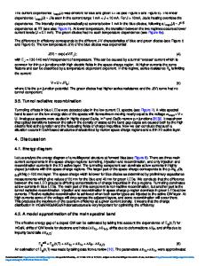
Structural Analysis in Low-V-defect Blue and Green GaInN/GaN Light Emitting Diodes Mingwei Zhu1,2, Theeradetch Detchprohm1,2, Yong Xia1,2, Wei Zhao1,2, Yufeng Li1,2, Jayantha Senawiratne1,2, Shi You1,2, Lianghong Liu3, Edward A. Preble3, Drew Hanser3, and Christian Wetzel1,2 1 Future Chips Constellation, Rensselaer Polytechnic Institute, 110 Eighth Street, Troy, NY, 12180 2 Department of Physics, Applied Physics, and Astronomy, Rensselaer Polytechnic Institute, 110 Eighth Street, Troy, NY, 12180 3 Kyma Technologies, Inc., 8829 Midway West Road, Raleigh, NC, 27617 ABSTRACT In this study, we characterized the structural defects in blue and green GaInN/GaN LEDs grown on c-plane bulk GaN and sapphire substrates. Low density large V-defects with diameters around 600 nm were found in the blue LEDs on bulk GaN. They were initiated by edge-type threading dislocations (TDs) around the homoepitaxial growth interface. On the other hand, a high density 7×109 cm-2 of smaller V-defects with sidewalls on {1 1 01} facets was observed in the active region of green LEDs on sapphire. Their diameter ranges from 150 to 200 nm. Misfit dislocations (MDs) generated in the quantum wells are found to initiate these V-defects. With optimizing the epitaxial growth conditions, the generation of MDs and their smaller V-defects was largely suppressed. As a result, the light output power improved by one order of magnitude. For green LEDs on bulk GaN, another unique type of defect was found in the active region: an inclined dislocation pair (IDP). In it a pair of dislocations propagate at a tilt angle of 18 to 23º from the [0001] growth direction towards < 1 1 00 > . This defect seems to be a path of strain relief in the high indium composition quantum wells. INTRODUCTION The group-III nitride material system has made rapid progress in recent years allowing the realization of light emitters in the UV and visible spectral range. High efficiency blue light emitting diodes (LEDs) have been demonstrated by using GaInN/GaN heterostructures. In order to achieve longer emission wavelength in the green and deep green spectral range, a higher InN fraction in the GaInN quantum wells (QWs) is essential. This, however, also results in a higher strain produced by the lattice mismatch between the GaInN well on the GaN template. Consequently, defects such as misfit dislocation (MD), stacking fault, V-defect, etc. could be created in the active region. For LEDs grown on sapphire, an additional high density of threading dislocations (TDs), generated at the sapphire/GaN interface, typically propagates into the active region. It is believed that by reducing the density of such defects and achieving higher lateral morphological homogeneity in the active region, the performance of green LEDs would be further improved.1 With recent advances of hydride vapor phase epitaxy (HVPE), bulk GaN with TD densities as low as 105 cm-2 provide an ideal template for homoepitaxial growth.2 Here we will use transmission electron microscopy (TEM) to analyze the structural
Data Loading...