Structural Analysis of Nanocrystalline Silicon Prepared by Hot-wire Chemical Vapor Deposition on Polymer Substrates
- PDF / 154,790 Bytes
- 6 Pages / 612 x 792 pts (letter) Page_size
- 87 Downloads / 354 Views
0989-A22-03
Structural Analysis of Nanocrystalline Silicon Prepared by Hot-wire Chemical Vapor Deposition on Polymer Substrates Michael M. Adachi1, Farhad Taghibakhsh1, Karen L. Kavanagh2, and Karim S. Karim1 1 School of Engineering Science, Simon Fraser University, 8888 University Drive, Burnaby, V5A 1S6, Canada 2 Department of Physics, Simon Fraser University, 8888 University Drive, Burnaby, V5A 1S6, Canada
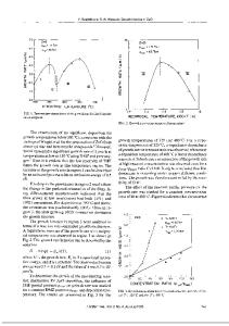
ABSTRACT Nanocrystalline silicon (nc-Si:H) films were deposited by hot-wire chemical vapor deposition (HWCVD) directly onto Corning glass and polyimide (Kapton E) substrates. The effect of silane concentration (in hydrogen carrier gas) on film crystallinity and conductivity were studied for a constant substrate growth temperature of 220 °C. Raman spectroscopy, X-ray diffraction and cross-sectional transmission electron microscopy (XTEM) showed that nc-Si:H (grain-size 20-65 nm) was observed for silane concentrations below 5.8 %. Similar to previous reports, closer inspection using XTEM found that there was an initial growth of an amorphous interfacial layer which then crystallized into a randomly-oriented polycrystalline material after 10 – 100 nm of growth. However, unlike previous reports, there was no detectable difference in the structure or conductivity for films grown on the two types of substrates. In both cases, the dark conductivity decreased with increasing silane concentration while the photo-conductivity was uniform for all films at values between 2 and 4×10⁻⁵ S/cm. INTRODUCTION Nanocrystalline silicon has gained considerable attention for use as the absorber layer in thinfilm silicon solar cells. This is due to stability against light induced degradation compared to hydrogenated amorphous Si (a-Si:H), and sensitivity in the near-infra red wavelengths. Films prepared by hot-wire chemical vapor deposition (HWCVD) [1], also known as catalytic chemical vapor deposition (CAT-CVD) [2], has gained interest due to the potential for high deposition rates and simple, large-area scale-up [3]. In addition, HWCVD facilitates low temperature deposition allowing films to be deposited onto flexible substrates such as polymer foils. Flexible substrates in turn facilitates roll-to-roll manufacturing, a means to reducing manufacturing costs for large area applications. Films grown by ECR plasma deposition have been reported to require an a-Si or Moly interlayer to grow crystalline films when deposited directly only polyimide substrate [4]. In this study, nc-Si:H films with high crystalline volume fractions were deposited by HWCVD on both Corning glass and polyimide substrates at silane concentrations near the known transition point between nanocrystalline and amorphous phases. Films were characterized by electrical conductivity measurements as well as structural analysis by x-ray diffraction (XRD), Raman spectroscopy and cross-sectional transmission electron microscopy (XTEM).
EXPERIMENT Amorphous and nanocrystalline films were deposited in a commercially available HWCVD chamber [5]. Two straight 10 cm Ta filamen
Data Loading...