Structural Defects and Their Relationship to Nucleation of GaN Thin Films
- PDF / 6,448,314 Bytes
- 12 Pages / 414.72 x 648 pts Page_size
- 108 Downloads / 266 Views
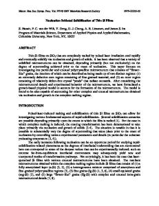
growth mode and the layer nucleation mechanism which was characterized by scanning force microscopy. Table I. Lattice parameters (in A) and thermal expansion coefficients (in K- 1 ) of wurtzite GaN, AIN and hexagonal (x-A1203 GaN
AIN
at-A1203
Lattice parameter
a c
3.189 5.178
3.111 4.979
4.758 12.991
Thermal exp. coefficient
a c
5.59x10- 6 3.17x10- 6
4.2x10- 6 5.3x10⁻⁶
7.5x10⁻⁶ 8.5x 10⁻⁶
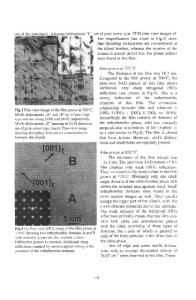
EXPERIMENTAL The GaN samples used in this study were grown on both (0001) and (1120) sapphire substrates using an inductively-heated, water cooled, vertical OMVPE reactor operated at 57 torr [19,20]. An AIN (or GaN) buffer layer, 200 to 500 A in thickness, was deposited at 450 °C to 550 'C before the high temperature deposition of GaN. TEM specimens were prepared by first lapping with diamond paste on a titanium plate down to a thickness of about 100 Jtm, followed by polishing with consecutively smaller size diamond pastes and/or alumina (A1203) in a Gatan dimpler down to a thickness of about 20 ýtm. The specimen was then sputtered to electron transparency by Ar+ at liquid nitrogen temperature. Transmission electron microscopy observations were carried out on a Philips EM420-TEM and a JEOL 4000 EX-TEM, operated at 120 keV and 400 keV, respectively. For surface observations, the as-grown films were examined in air with a Park Scientific Instruments scanning force microscope. The 5 [tm scanner was operated at 2 Hz. All images were acquired in the constant force mode using 3 to 12 nN of contact force. RESULTS Crystalline Orientation and the Interface GaN epitaxial layers grown on both c-plane and a-plane (x-A1203 substrates crystallize with the wurtzite structure and the growth is along the c-axis. The crystal orientation relationships of GaN and AIN grown on sapphire substrates are summarized in Table II. Selected area electron diffraction (SAD) and high resolution electron microscopy reveal that both GaN and AIN layers grow epitaxially on their substrates. For growth on (0001) (x-A1203, the epitaxial relationships were determined to be: (OOO)GaN//(0001)AIN//(0001)a-AI203, with in-plane orientation relations of [ l TOO]GaN//[ 1OO0]A1N//[ 112 0]l-A1203, in agreement with previously published results [ 15, 21]. For growth on (1120) oc-A1203, both GaN (0001) and AIN (0001) planes were found to be parallel to the (1120) substrate plane, with in-plane orientation relations of [1T-00]GaN //[1lTOO]A1N//[0001]xA1203,in accordance with observations by other groups [12, 22,23].
476
Table II. Epitaxial relationships during growth of GaN, AIN on c- and a-plane sapphire Growth direction
In-plane orientation relationship
Epilayer
Substrate
Epilayer
Substrate
(0001)GaN (0001)A1N
(0001) x-A1203
[1100] GaN [ 1TOO] AIN
[1120] a-A1203
(0001) GaN
(112-0) a-A1203
[ 1Too] GaN
[0001] a-A1203
(0001) AIN
[I TOO] AIN
The interface between the AIN (or GaN) buffer layer and the sapphire substrate was found to be locally coherent and the misfit dislocation spacing is almost uniform. Figure 1 shows the TEM micrographs of the AIN/(
Data Loading...