Comparative Study of Typical Defects in III-Nitride Thin Films and Their Alloys
- PDF / 2,212,570 Bytes
- 6 Pages / 414.72 x 648 pts Page_size
- 66 Downloads / 244 Views
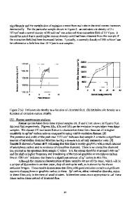
In the recent years, III-Nitrides have generated tremendous interest primarily due to the possibility of using them in light-emitting diodes and lasers operating in blue and ultraviolet region. The wurtzite polytypes of GaN, AIN, and InN form continuos solid solutions and thus direct bandgaps can be tailored from 1.9 eV (InN) to 3.4 eV (GaN) to 6.2 eV (AIN). In view of the these exciting technological applications, there is a need to grow these materials in the form of device quality thin films on practical substrates such as silicon and sapphire. The lifetime of the currently used devices based on III-V phosphides, and also II-VI semiconductors is strongly related to the densities of dislocations in the active region [1,2]. Even moderate dislocation densities (_ 104 cm 2 ) decrease the operating life of these devices. The role of these defects during the operation of IIINitrides heterostructures is not clear at this time. Some studies [3] show that the optical properties and lifetimes of the GaN-based LEDs are remarkably insensitive to structural dislocations and little degradation has been observed to occur in spite of the extremely high densities of dislocations (108-10" cm-). However, depending on the growth method and specific growth conditions, different types of two-dimensional defects (inversion domain boundaries, stacking faults) and dislocations with various Burgers vectors might be present in HII-Nitride films, which can have different effects on the electrical/optical properties. Therefore, a careful study of the type of dislocations and two-dimensional defects present in the films as a function of growth conditions, and further correlation with the electrical/optical properties are necessary in order to understand the role of these defects on device characteristics. 411 Mat. Res. Soc. Symp. Proc. Vol. 482 0 1998 Materials Research Society
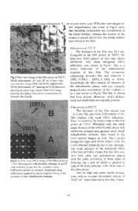
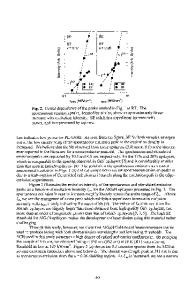
EXPERIMENTAL The GaN and GaN/GaAIN heterostructures were grown on the basal (0001) plane of sapphire by MOCVD technique using 350-500 A buffer layers of AIN. The films (0.6 - 0.9 l.m thickness) were grown in a horizontal low pressure metalorganic chemical vapor deposition reactor. Details of the growth are reported elsewhere [4]. The following growth conditions were found to be optimum for the growth of device-quality films: the growth temperature of 10000 C, the growth pressure 10 mbar. The flow rates were about 20Amol/min for TMGa and 1000 cc/min for NH 3, resulting in a growth rate of 0.7 p.m/h as determined by ball polishing. The GaN, GaN/GaAIN and GaAIN/GaN heterostructures obtained under different growth conditions were studied by transmission electron microscopy (TEM). Conventional TEM planview and cross-sectional sample preparation technique consisting of mechanical polishing and Ar ion milling at 6.5 kV (and 2 kV at the final stage) was used. TEM studies were carried out on a Topcon 002 B transmission electron microscope operated at 200 kV. RESULTS We have carried out thorough TEM investigations of GaN, GaA1N/GaN and GaN/GaAlN films grown on basal (0002) pl
Data Loading...