Structural, optical and photocatalytic properties of pure and Pd-doped CdS thin films
- PDF / 1,712,033 Bytes
- 11 Pages / 595.276 x 790.866 pts Page_size
- 21 Downloads / 352 Views
Structural, optical and photocatalytic properties of pure and Pd-doped CdS thin films Syed Mansoor Ali1 · M. A. Majeed Khan2 · Turki S. ALKhuraiji3 Received: 18 March 2020 / Accepted: 20 July 2020 © Springer Science+Business Media, LLC, part of Springer Nature 2020
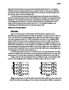
Abstract Pure and palladium (Pd)-doped cadmium sulfide (CdS) thin films were deposited on glass substrate by successive ionic layer adsorption and reaction (SILAR) process with different doping concentrations. X-ray diffraction results confirmed the crystalline and hexagonal phase structure of prepared samples. The increase in the main diffraction peak (002) intensity with d+2 in the lattice. The crystallite size increased from increasing Pd concentration revealed the substitution of P d+2 with C 58.32 to 89.71 nm with Pd concentration. Morphology of the thin films shown that the average grain size increases by the agglomeration of nano-grains which become cluster of particles after P d+2 incorporation. The energy bandgap of the CdS thin films is decreased from 2.44 to 2.37 eV with increasing Pd percentage. Photoluminescence (PL) spectra described that the pure and Pd-doped thin films show a broad PL emission peak associated to the transition of sulfur ion vacancy transfers to the valence band. Moreover, the Pd doping improved the film photostability as well as the photocatalytic degradation of methylene blue (MB).
1 Introduction Cadmium sulfide is a significant II–VI wide bandgap (∼2.42 eV) compound semiconductor with a direct transition. Due to its versatile properties like low work function, thermal stability, good optical transparency and electronic charge mobility [1], CdS have promising future applications such as hydrogen production [2], field-effect transistor, lightemitting diode [3], gas sensors [4], wastewater treatments [5, 6], transistors [7], waveguides [8], solar cells [9], photodetectors [10] nano-generators [11], photocatalysis [12] and photo-electrochemical sensors [13]. The CdS thin-film properties can be significantly tuned by doping, which is attributed to the structural defects or sulfur vacancies and cadmium interstitials [14, 15]. Accordingly, it is a promising material to control the properties by introducing an * Syed Mansoor Ali [email protected]; [email protected] 1
Department of Physics and Astronomy, College of Science, King Saud University, P.O. BOX 2455, Riyadh 11451, Saudi Arabia
2
King Abdullah Institute for Nanotechnology, King Saud University, Riyadh 11451, Saudi Arabia
3
National Center for Irradiation Technology, King Saud University, Riyadh, Saudi Arabia
appropriate dopant. Numerous researches have been made to synthesize CdS thin films with dopant ions such as Cu2+ [15] In3+ [16], B3+ [17], Ni2+ [14] and A l3+ [18] to improve the structural, optical and electrical properties. However, based on the literature P d2+-doped CdS thin films with SILAR technique have not been investigated. Pure and doped CdS thin films are prepared through variety of techniques, such as spray pyrolysi
Data Loading...