Structural studies of diamond thin films grown from dc arc plasma
- PDF / 703,834 Bytes
- 10 Pages / 612 x 792 pts (letter) Page_size
- 105 Downloads / 280 Views
MATERIALS RESEARCH
Welcome
Comments
Help
Structural studies of diamond thin films grown from dc arc plasma L. C. Nistora) and J. Van Landuytb) EMAT, University of Antwerpen, Groenenborgerlaan 171, B 2020 Antwerpen, Belgium
V. G. Ralchenko, A. A. Smolin, K. G. Korotushenko, and E. D. Obraztsova General Physics Institute, ul. Vavilova 38, Moscow 117942, Russia (Received 1 August 1995; accepted 20 June 1997)
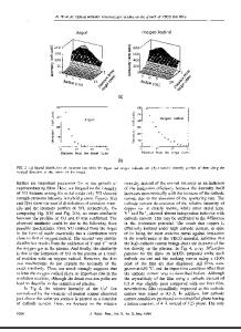
Diamond thin films grown from a dc-arc discharge in CH4yH2 mixtures on Si wafers were examined by transmission electron microscopy and Raman spectroscopy. This deposition method provides good diamond crystallinity at high CH4 concentrations (3% –9%). Seeding the substrate with 5 nm diamond particles at a density of 2 3 1012 cm 21 followed by argon laser irradiation to reduce their agglomeration gives, just after starting deposition, a density of growth centers of 1010 cm22 . At 3% CH4 concentration the film grows with almost perfect crystallites. Richer CH4 mixtures (5% and 9%) produce crystallites with twins and stacking faults. An amorphous 20 –70 nm SiC interlayer is present at these CH4 concentrations, which was not observed at 3% CH4 . Amorphous sp 3 - and sp 2 -bonded carbon was detected by Raman spectroscopy at all CH4 concentrations and correlated with TEM data.
I. INTRODUCTION
The recent progress in growth of polycrystalline diamond thin films by chemical vapor deposition techniques makes this material with outstanding properties available for practical applications (see, for example, Ref. 1). Currently more than 10 methods of diamond synthesis at low pressure are used, the microwave plasma and hot filaments being the most common methods to excite methane-hydrogen mixtures. The structure of carbon deposits strongly depends on the deposition conditions, varying from graphitic carbon to high quality diamond with a minimum number of defects and non-diamond phase inclusions. The quality of the asgrown diamond films is a critical issue for their use in particular applications, especially in optics and electronics. The study of internal structure, defects, and impurities, which are created during CVD diamond growth, is important also for the better understanding of the nucleation and growth mechanisms at various experimental conditions. Transmission Electron Microscopy (TEM) is a powerful analytical tool for detailed investigation of the microstructure of CVD diamond.2 However, because of the time-consuming procedure of sample preparation for TEM examination requiring dedicated instrumentation and specific know-how, this technique is not as a)
On leave from the National Institute of Materials Physics, I.F.T.M., P.O. Box Mg-6 Magurele, 76900 Bucharest, Romania. b) Author to whom correspondence should be addressed. J. Mater. Res., Vol. 12, No. 10, Oct 1997
http://journals.cambridge.org
Downloaded: 19 Nov 2014
commonly used by researchers involved in diamond synthesis as, for instance, is Raman spectroscopy. A number of authors reported TEM studies on diamond thin films grown on Si substrates by differ
Data Loading...