Structure and Novel Electrical Effects in A-Si:H Based Multilayers Containing Discontinuous Metal Sublayers
- PDF / 1,301,982 Bytes
- 6 Pages / 414.72 x 648 pts Page_size
- 20 Downloads / 255 Views
Mat. Res. Soc. Symp. Proc. Vol. 382 01995 Materials Research Society
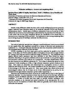
Figure 1. Left-shaded SFM micrograph of a Mo/a-Si:H bilayer system containing a molybdenum sublayer with a nominal thickness of 0.6 nm. The average height of the band-shaped metal structures amounts to about 8 nm.
a thickness of 80 nm. The deposition parameters chosen were those for optimized highly photoconductive a-Si:H [2]. The nominal thickness of the metal sublayers determined from the deposition rate for thick films and deposition time was varied between 0.4 nm and 9.8 nm. The other set of samples contained only one metal sublayer (msp molybdenum or thermally evaporated vanadium) arranged between two a-Si:H sublayers, which were deposited by if-glow discharge technique (gd). Investigations of surface topology were performed on the top layers of the a-Si:H/metal/a-Si:H triple-layers at various stages of the sample deposition by scanning force microscopy (SFM) and spectroscopic ellipsometry in the energy range from 1 eV to 5 eV. Moreover, the structure of the multilayers was investigated by cross-sectional transmission electron microscopy (TEM). The electrical measurements were performed using a coplanar electrode arrangement with sputtered NiCr stripe contacts of 10 mm length and 0.5 mm interelectrode spacing. Measurements of the temperature dependent conductivity were carried out in a cryostat at temperatures between 90 K and 430 K. The conductivity (or better the normalized current density in the case of a non-ohmic current-voltage dependence) was determined by a = j/E, were j and E are the current density and the electric field. Investigations of the current-voltage I(U)-characteristics and the time dependence of the current I(t) of Mo/a-Si:H bilayers were performed in-situ on growing molybdenum top layers. Each measurement cycle was started with recording the I(U)-characteristic. It was continued by the record of the I(t)-data at the maximum voltage applied in the preceding I(U)-measurement. From one to the following measuring cycle the maximum applied voltage was increased by steps of 5 V in the range from 5 V to 20 V. All I(t)-measurements were carried out over a period of 10 min with a time resolution below 0.13 s.
272
101
Met/a-Si:H- MLS
10°0
10"1 102 10.
5
10-4
bD10-6 7
10.
1o-S
Metal ATi
10-9 o Mo 10_10 11 V
0.04
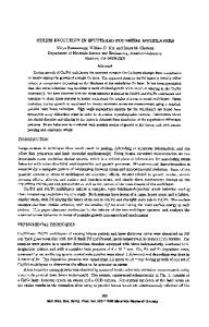
d.(nm) T0 (K)3_ 3.1.103 1.1 0.4 0.4
0.06
4.1.10
4.3. 10
,
0.08 T-" 2(K-" 2)
0.10
0.12
Figure 2. Semi-logarithmic plot of the conductivity a versus the square root of the inverse temperature T for triple-layers and a multilayer (Ti/a-Si:H) containing discontinuous metal sublayers with the nominal thickness d•,. The characteristic temperatures To were determined by fitting the data to eq. 1. STRUCTURE AND ELECTRICAL PROPERTIES Fig. 1 displays a left-shaded scanning force micrograph of the surface of a molybdenum top layer on a 65 nm thick layer of gd a-Si:H. The nominal thickness of the molybdenum layer was determined to 0.6 nm. The surface of the sample presented in Fig. 1 consists of elevated band-
Data Loading...