Structure of Chemically Passivated Semiconductor Surfaces Determined Using X-Ray Absorption Spectroscopy
- PDF / 1,327,327 Bytes
- 12 Pages / 417.6 x 639 pts Page_size
- 52 Downloads / 271 Views
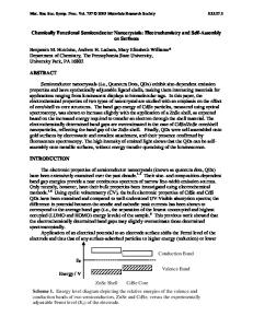
powerful in the study of dilute dopant systems. Partial or total electron yield (TEY) detection techniques, which intrinsically have a very high surface sensitivity (a few 100 nm in TEY versus several microns for FY at the 2-4 keV energy range used here), might be expected to be well suited to studies of monolayer adsorbate systems, such as those important in semiconductor passivation. The intrinsic surface sensitivity is why we devoted a lot of our effort in the general area of semiconductor XAFS to various types of TEY detection [23,24]. However, especially at higher energy edges, the background from the substrate poses significant problems to electron detection, particularly TEY. Also, diffraction artifacts in TEY of single crystal semiconductors are often as challenging as those in FY detection [25]. For these reasons energy dispersive FY detection offers numerous advantages to TEY, especially when an array detector with high angular acceptance, high efficiency and high energy resolution is used. Figure 1 compares the fluorescence yield
(FY) and total electron yield (TEY) signal from
b) TEY - raw signal (true 0))
CI/GaAs(1 11) recorded simultaneously. Relative to the TEY spectrum, FY detection gives an enormous improvement in signal to background. x -This makes FY much less sensitive than TEY to systematic noise, even though the TEY signal is X1 much larger, in part because Auger yields are -10 "A c)TEY background subtracted times greater than FY in this regime, and in part . because of signal amplification by secondary electron generation. Clearly, the ability of energy > filtered X-ray fluorescence detection to collect almost all of the adsorbate signal with very high a) FY raw - signal (true 0) discrimination against substrate signal makes it superior for most adsorbate and thin film studies. FY has significant disadvantages with concentrated thick film or bulk samples where absorption ICVGaAs(111) - A saturation [26] distorts the signal, or where there is overlap of substrate and analyte fluorescence, as in 0 , , , InP-S. 2800 2900 3000 3100 3200 3300 Photon Energy (eV) Here we report studies of Ge(1 11)-Cl; GaAs( 111)-Cl; GaAs(001)-S, GaAs( 1Il)A-S, and Fig.1 Comparison of simultaneously recorded GaAs(1 I1)B-S passive layers prepared by solution fluorescence yield (FY) and total electron yield chemistry. Although not directly relevant to (TEY) Cl Is X-ray absorption spectra of passivation of compound semiconductor surfaces, GaAs(1 I1)A-Cl. Curves (a) and (b) are raw data with a true zero. Curve (c) is the TEY after the Cl/Ge(1 11) and Cl/GaAs(I 11) results [27] background subtraction and 100-fold illustrate our procedures, including the use of firstamplification. principles structure calculation. The results on GaAs-S extends earlier studies of this surface by many different techniques including theory [28], RHEED [29,30], XPS [31,32], XSW [30] and XAFS [31,33,34]. Surfaces prepared using brief exposure at 25°C to a (NH4) 2Sx solution followed by a water rinse, without annealing, are found to produce a
Data Loading...