Study of annealed Indium Tin Oxide Films Prepared by RF Reactive Magnetron Sputtering
- PDF / 397,567 Bytes
- 6 Pages / 414.72 x 648 pts Page_size
- 11 Downloads / 488 Views
" Thankful
to the Funda•,io Luso-Americana para o Desenvolvimento for providing a
travel grant for this meeting. 379
Mat. Res. Soc. Symp. Proc. Vol. 388 01995 Materials Research Society
1
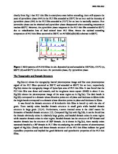
0.15 0 C,
6
0.1
04
5-.. C"-
0.05 --0-1(222)/1(440) K22- /1(400)
F4
0
100
0
200
300
400
500
Annealing Temperature ( °C) Fig. 1. The variations of peak intensity ratios of I (222)/I (400) and I (222)/1 (440) as a
function of the annealing temperature. RESULTS AND DISCUSSIONS Structural Properties The XRD patterns of the ITO films contain only In 20 3 peaks (10). All the films show the (400) plane texturing. The (002) peak intensity increases as the annealing temperature is increased although all the films have (400) preferred orientation. Figure 1 shows the variations of the 1 (222)/1 (400) and 1 (222)/I (440) with annealing temperature. It is clear that the intensity ratio increases as the annealing temperature is increased. The (400) diffraction peak width was used to estimated the crystallite dimension along the a axis (11). The results are shown in Fig.2 (a). It can be seen that the grain size along (400) direction increases as the annealing temperature is increased up to 300 "C and no clear variation after the annealing temperature is over than 300 "C. The (400) crystal plane distance was 2.54 T(b)
160 T (a) E e
*
"N 150+-C
*
*
e
S
2.53
I-
140
2.52
0 100 200 300 400 500 Annealing temperature ( *C)
I
I
0 100 200 300 400 500 Annealing temperature (°C) Fig.2.(b) d-values of ITO films vs. annealing temperature. The line gives the d-value of InO, powder.
Fig. 2. (a) Grain size of ITO films vs. annealing temperature.
380
Glass Substrate
100 100 ~~
Gls Sbtrt 0
500 0f 200
600
1000
1400
1800
2200 2600
Wavelength (nm)
Fig. 3. Specular transmittance spectra of ITO films asdeposited and annealed at different temperatures.
calculated from the diffraction angle which has been obtained by fitting the diffraction peak. The results are shown in Fig. 2 (b). The line in the figure is the standard value d, (2.529 A). It shows that the d values of all the films are larger than d,. However, as the annealing temperature is increased, the difference between the standard value and the calculated value becomes small. That means that there are compressive stress in all the films and the stress value decreases as the annealing temperature is increased. The SEM photographs of ITO films show that all the films have columnar structures. The average crystallite size along the sample surface is about 100 nm and no clear variation for the films annealed at different temperatures. This crystallite size is smaller than that along the direction normal to the sample surface estimated by XRD method. From SEM it can also be seen that the voids between the crystallite grain become small as the annealed temperature is increased. That means the annealing improves the film density. In addition, as the annealing temperature is increased, the film surface becomes rough which can improve the efficiency of amorphous silicon s
Data Loading...