Study of copper-refractory metal interfaces via solid-state wetting for emerging nanoscale interconnect applications
- PDF / 196,241 Bytes
- 8 Pages / 612 x 792 pts (letter) Page_size
- 69 Downloads / 317 Views
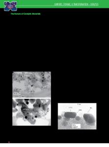
Solid-state wetting experiments were carried out to derive the work of adhesion (adhesion energy) of pertinent Cu/liner interfaces via the Young–Dupré equation using contact-angle measurements of the Cu equilibrium crystal shape on Ta and TaNx liners. Four types of liner surfaces were examined: untreated sputtered Ta (uSp-Ta), untreated sputtered TaNx (uSp-TaN), untreated atomic layer deposited (ALD) TaNx (uALD-TaN), and indium surfactant-treated ALD TaNx (tALD-TaN). All Cu-liner stacks were subsequently annealed at 600 °C for 48 h in a forming gas (95% Ar/5% H2) ambient. For Cu/uSp-Ta, the work of adhesion was found to be 2170 mJ/m2, corresponding to an average contact angle of 74°, while for Cu/uSp-TaN, the work of adhesion amounted to 1850 mJ/m2 for an average contact angle of 85°. Alternatively, the work of adhesion for Cu/uALD-TaN was determined to be 1850 mJ/m2, corresponding to an average contact angle of 85°, while for Cu/tALD-TaN, the work of adhesion was 2280 mJ/m2, at an average contact angle of 70°. These findings indicate that the highest degree of surface wetting occurs for the indium surfactant-treated ALD TaNx. It is thus suggested that surfactant treatment causes a reduction in the energy barrier to Cu nucleation, resulting in an enhancement in Cu wetting characteristics and a more uniform concentration of Cu nucleation sites. A critical potential outcome is the formation of atomically smooth Cu-liner interfaces with enhanced adhesion characteristics.
I. INTRODUCTION
The conductivity of polycrystalline metallic conductors used in integrated circuitry (IC) is influenced by several intrinsic (physical) and extrinsic (morphological) effects related to the conductor material. More specifically, as the cross section of the conductor approaches the bulk mean free path for electron scattering (39.3 nm for copper), the behavior of conduction electrons transitions from discrete, particlelike, to wavelike behavior. The transition increases the probability for electron scattering from the external boundaries of the metal wires, leading to a gradual rise in resistivity.1,2 This quantum mechanical driven phenomenon is further compounded by extrinsic scattering events from the internal grain boundaries within the polycrystalline matrix of the conductor, which further contribute to nonelastic scattering of carriers. Clearly, the combination of both scattering mechanisms present significant challenges in terms of
a)
Address all correspondence to this author. e-mail: [email protected] DOI: 10.1557/JMR.2006.0040 J. Mater. Res., Vol. 21, No. 1, Jan 2006
maintaining the current density levels required in emerging IC device nodes as copper (Cu) interconnect line widths are scaled down below a dimensional threshold estimated be in the 100–45 nm range.3–5 In this respect, the morphological scattering effects may be significantly mitigated through optimization of the properties of the interface between copper and the underlying diffusion barrier/liner. Such optimization would ensure the minimization of the e
Data Loading...