Study of electron beam irradiation induced defectivity in mono and bi layer graphene and the influence on Raman band pos
- PDF / 855,949 Bytes
- 6 Pages / 612 x 792 pts (letter) Page_size
- 74 Downloads / 334 Views
1184-HH03-07
Study of electron beam irradiation induced defectivity in mono and bi layer graphene and the influence on Raman band position and line-width G. Rao1, S. Mctaggart1, J. L. Lee1, and R. E. Geer1 1 College of Nanoscale Science and Engineering, University at Albany, SUNY, Albany NY 12222.USA
ABSTRACT
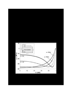
Nanoscale metrology of graphene-based devices is a substantial challenge. The investigation of defects and stacking order is essential for graphene-based device development. Raman spectroscopy is a useful approach in this regard. The defect-induced Raman D band yields substantial insights regarding defect density and, consequently, can serve as in important tool to quantify impact of defects on eventual graphene-based device performance. Toward this end an investigation of electron beam-induced defects in bi-layer and mono layer graphene samples has been undertaken via the examination of the Raman D, and G bands. The evolution of the aforementioned Raman spectra as a function of electron beam dose was characterized via Raman spectroscopy and compared with spectra from the same samples prior to irradiation. Defect generation in the graphene as a function of electron beam dose was characterized via the change in the intensity ratios of the Raman D and G bands (ID/IG) and the broadening of the G band line width. Continued irradiation at very high flux and very low accelerating voltages have also revealed charge accumulation evident from the narrowing of G band line-widths. INTRODUCTION Graphene, a two-dimensional hexagonal, sp2 coordinated array of carbon atoms provides new possibilities for post-CMOS electronics1,2. Graphene exhibits remarkable electronic properties including ballistic carrier transport with room temperature carrier mobilities as high as 20 000 cm2/Vs1,3.The linear electronic dispersion of graphene is postulated to imbue charge carrier behavior akin to Dirac-Fermions4. However, the presence of edge defects and disorder in the material has been shown to degrade these properties. It has been reported that edge defects and disorder reduces the mobility to 3000-5000 cm2/Vs5. Since defects and lattice distortion in graphene can be introduced via energetic charged particles it is essential to characterize the effects of characterization or device fabrication tools employing such (e.g. SEM, TEM , FIB EB Litho, etc…). Defect formation has been observed earlier in carbon nanotubes with electron irradiation in a SEM. Very low accelerating voltages (~0.5, 1kV) have proved to induce more extensive damage6. The induced defectivity increased electron scattering in the CNT material thereby reducing overall electron mobility7. Consequently, the work presented here has focused on the effects of very low energy electron irradiation on mono (1L) and bi (2L) layer graphene samples. It is observed that electron irradiation results in increased defect formation in both 1L and 2L graphene per the variation of the Raman D/G intensity ratio. Considering the energy spectrum of the radiation, the increased
defect sign
Data Loading...