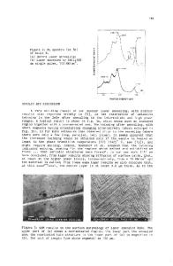
Study of the Surface Morphology, Electrophysical Characteristics, and Photoluminescence Spectra of GaAs Epitaxial Films
- PDF / 993,349 Bytes
- 8 Pages / 612 x 792 pts (letter) Page_size
- 51 Downloads / 274 Views
TROSCOPY OF CONDENSED PHASES
Study of the Surface Morphology, Electrophysical Characteristics, and Photoluminescence Spectra of GaAs Epitaxial Films on GaAs(110) Substrates G. B. Galieva, E. A. Klimova, A. A. Zaitsevb, S. S. Pushkareva, *, and A. N. Klochkova a
Mokerov Institute of Ultrahigh Frequency Semiconductor Electronics, Russian Academy of Sciences, Moscow, 117105 Russia b National Research University “MIET”, Zelenograd, Moscow, 124498 Russia * e-mail: [email protected] Received December 17, 2019; revised January 15, 2020; accepted February 28, 2020
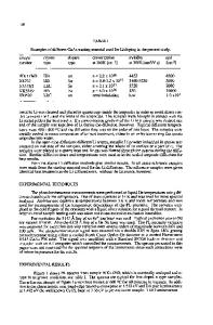
Abstract—The electrophysical and phosphorescence characteristics, as well as the surface morphology, of GaAs films grown by molecular beam epitaxy on GaAs substrates with the (110) crystallographic orientation are studied. The silicon-doped epitaxial layers were grown at temperatures from 410 to 680°C with arsenicto-gallium flux ratios from 14 to 84. The ranges of the growth conditions for obtaining the smoothest epitaxial film surface are determined by atomic force microscopy. The behavior of silicon atoms in GaAs is interpreted using analysis of the photoluminescence spectra of the grown samples taking into account that silicon atoms occupy Ga or As sites, i.e., taking into account the appearance of SiGa and SiAs point defects, as well as of arsenic and gallium vacancies VAs and VGa. Keywords: GaAs(110), molecular beam epitaxy, photoluminescence spectroscopy, amphoteric nature, surface morphology DOI: 10.1134/S0030400X20070061
INTRODUCTION 3B5
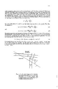
semiconductor compounds epitaxially The A grown on substrates with the (100) crystallographic orientation are most widely used in modern microelectronics and best studied. This is partly related to the fact that molecular beam epitaxy (MBE) allows one to rather easily grow a large number of various structures on these substrates for different applications. However, in recent years interest has grown in structures grown on substrates with (111) and (110) orientations. The delay in the application of these substrates is caused by the relatively narrow range of technological conditions of epitaxial growth on these substrates in comparison with the growth on (100) substrates [1]. The main growth parameters are (i) growth temperature, (ii) partial pressure ratio of the III and V group elements, and (iii) growth rate. However, it was shown in recent years that semiconductor structures grown on (111)A and (110) substrates are promising for creating a new generation of field transistors, as well as of original quantum-well structures, topological insulators, etc. [1]. In addition, structures on (111)А and (110) substrates possess a built-in piezoelectric field directed vertically or lying in the growth plane [2–4]. This circumstance affects not only the mechanism and specific features of epitaxial growth, but also the fun-
damental properties of the grown structures [1]. It is also well known that silicon as a doping impurity exhibits pronounced amphoteric properties in GaAs epitaxial films grown on (111)А and (110) GaAs subs
Data Loading...