Photoluminescence Spectra of C + -Implanted GaAs: Experimental Verification on Amphoteric Features of Carbon Impurities
- PDF / 443,231 Bytes
- 6 Pages / 420.48 x 639 pts Page_size
- 76 Downloads / 348 Views
PHOTOLUMINESCENCE SPECTRA OF C+-IMPLANTED GaAs: EXPERIMENTAL VERIFICATION ON AMPHOTERIC FEATURES OF CARBON IMPURITIES IN GaAs YUNOSUKEEMA•ITA*, SHIGMU SHIGET•**, MASAHIKO MORI*, NOBUKAZU OHNISHI***,
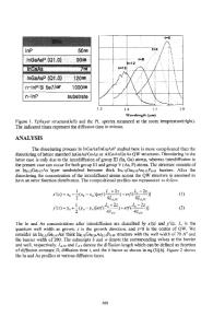
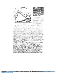
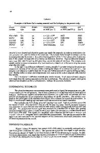
PAU P•ELAN and TOKUE MATSUMORI Electrotechnical Laboratory, 1-1-4 Umezono, Tsukuba-shi, Ibaraki-ken 305, Japan Department of Physics, Kurume University, 1635 Mii-machi, Kurume-shi, Fukuoka-ken 830, Japan Institute of Fundamental Analysis Inc.,Ltd., 3-24-3 Yoyogi, ****Shibuya-ku, Tokyo 151, Japan Department of Electronics, Tokai University, 1117 Kitakaname, Hiratsuka-shi, Kanagawa-ken 259-12, Japan ABSTRACT C+ ion-implantation was carried out for extremely pure GaAs gown by moleplarIeam epitaxy. The dose was very widely varied from 1x10⁹ to 1x10 cm -. Photoluminescence and Raman scattering measurements were performed at 2 K and room temperature, respectively, both as functions of dose and jneal ng temperature. The results revealed that for a dose less than 5x10" -cm- , where the dominant damages are point defects, annealing at 200 °C is sufficient to attain a damage-free lattice. When the dose is above that value, where the principal damage is a highly disordered lattice, annealing, at least above 550 °C, is required. Photoluminescence spectra showed that the well-defined near-band-gap emission, [g-g], (exclusively inherent to acceptors), was a dominant emission in the above mentioned low dose region, but was strongly suppressed in the higher region. These observations indicate that ion-implanted C atoms in GaAs behave as a~hote5 ic impurities when the dose exceeds a critical value, of around 5x10 cm- . INTRODUCTION When GaAs is prepared by molecular beam epitaxy (MBE), C is a most difficult element to eliminate [l]. It is then prerequisite to collect detailed data on C, in order to grow high-quality GaAs. Information on amphoteric impurities like C and Ge is quite unsatisfactory as yet. Of the various ways to dope impurities, either during or after crystal growth, ion beams are supposed to be the only practical method. Using ion implantation we recently introduced C into GaAs [1]. Low-temperature photoluminescence (PL) spectra of these samples revealed that C atoms form plural new emissions near the band-edge. Among these, [g-g] was found to be observed Just below t0g boiud exciton emissions when the dose of C atoms, [C] is larger than ilO cmHI Ameng many optical measurements Raman scattering is a very powerful method to evaluate the degree of crystalline recovery from the damaged state [2]. The purpose of the present paper is to get extensive information on the optical properties oS C ion-implanted GaAs for an extremely wide range of [C] up to 1x1O'- cm- . We here present combined data between PL and Raman scattering as functions of both [C], and annealing temperature, TA, and suggest that C atoms in GaAs should behave as amphoteric impurities. EXPERIMENTAL For ion-implantation, undoped (UD-) GaAs, which was grown on (100) substrates by MBE at 550 °C, was used. Judflng f~om PL spectra the residyal impurity concentrati
Data Loading...


