Study on the Polycrystalline Silicon Films Deposited by Inductively Coupled Plasma Chemical Vapor Deposition
- PDF / 1,057,322 Bytes
- 6 Pages / 595 x 842 pts (A4) Page_size
- 79 Downloads / 436 Views
Study on the Polycrystalline Silicon Films Deposited by Inductively Coupled Plasma Chemical Vapor Deposition Byeong Y. Moon, Jae H. Youn, Sung H. Won, Jin Jang and Stanislaw M. Pietruszko1 Department of Physics and Department of Information Display, Kyunghee University, Seoul, 130-701, Korea 1 Warsaw University of Technology, Institute of Microelectronics and Optoelectronics, IMiO PW, ul. Koszykowa 75, 00-662 Warsaw, Poland
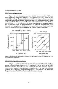
ABSTRACT Polycrystalline silicon thin films have been deposited by an inductively coupled plasma chemical vapor deposition using SiH4/H2 mixtures. The quality of poly-Si can be improved by increasing RF power and hydrogen dilution ratio. The poly-Si deposited at a RF power of 1000 W with an addition of H2, showed a Raman polycrystalline volume fraction of 85.7 %, FWHM of 6.4 cm-1, deposition rate of 9.64 Å/s and SEM grain size of ~3000 Å.
INTRODUCTION Polycrystalline silicon (poly-Si) has attracted much attention because of its wide range of applications in large-area electronics, such as solar cell, thin film transistor (TFT), image sensor, etc. Solid phase crystallization (SPC) is one of the common methods to crystallize amorphous silicon (a-Si). The SPC produces a large grain size but its crystallization temperature is too high for use of glass substrates [1,2]. In order to reduce the crystallization temperature, laser annealing is used to recrystallize a-Si [3,4]. The advantages of this method are that there is no damage to the glass substrate and the poly-Si obtained has a good crystallinity with very few in-grain defects, due to the melt-regrowth process. However, there are technological problems to be solved for large-area applications. One is a small grain size due to high solidification velocity. The other is the non-uniformity of the material especially in the laser overlap region, which is serious for applying this material to large-area devices. The best way, therefore, will be a direct deposition of poly-Si from gas plasma at a temperature low enough to utilize inexpensive large-area glass substrate [5]. Plasma chemical vapor deposition (CVD) using capacitively coupled plasma (CCP) has been widely used for deposition of silicon film. Several problems remain to be solved for further improvement of the performance and characteristics of poly-Si based devices, i.e. low deposition rate, powder formation and poor crystallinity at the early stage of growth. In addition, radicals and ions in plasma give rise to various damages in the deposited semiconductor film [6,7]. Various high-density plasma sources such as electron cyclotron resonance (ECR), helicon wave and inductively coupled plasma (ICP) CVD have been developed. The ICPCVD has a high electron density of about 1012 cm-3 at 10 mTorr, whereas a capacitively coupled plasma using parallel plates shows a density of around 1010cm-3 [8]. The ICP source offers additional advantages of simple design, good uniformity without external magnets and lower ion bombardment on the growing surface than conventional planar type sources.
D5.2.1
EX
Data Loading...