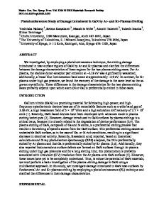
Surface Damage Introduced by Diamond Wire Sawing of Si Wafers: Measuring in-depth and the Lateral Distributions for Diff
- PDF / 318,727 Bytes
- 6 Pages / 432 x 648 pts Page_size
- 45 Downloads / 305 Views
Surface Damage Introduced by Diamond Wire Sawing of Si Wafers: Measuring in-depth and the Lateral Distributions for Different Cutting Parameters Bhushan Sopori,1 Srinivas Devayajanam,1,2 Prakash Basnyat,1,2 Rekha Schnepf,1 Santosh Sahoo1,2 James Gee,3 Ferdinando Severico,3 Hubert Seigneur,4 Winston V. Schoenfeld,4 Steve Preece,4 Jeff Binns,5 Jesse Appel,6 and Kaitlyn VanSant1 1
National Renewable Energy Laboratory, Golden, CO 80401, USA
2
New Jersey Institute of Technology, Newark, NJ 07102, USA
3
Applied Materials, Santa Clara, CA 95054, USA
4
PVMC, Orlando, FL 32826, USA
5
SunEdison, Portland, OR 97216, USA
6
SunEdison, St Peters, MO 63376, USA
ABSTRACT This paper describes the characteristics of damage, introduced under different conditions of diamond wire sawing, on the Si wafer surfaces. The damage occurs in the form of frozen-in dislocations, phase changes, and microcracks. The in-depth damage was determined by conventional ways such as TEM, SEM and angle-polishing/defect-etching, which only provide local information. We have also applied a new technique based on sequential measurement of the minority carrier lifetime after etching thin layers from the surfaces to determine average damage depth and its in-depth distribution. The lateral spatial damage variations, which seem to be mainly related to wire reciprocation process, were observed by photoluminescence and lifetime mapping. Our results show a strong correlation of damage depth on the diamond grit size and wire usage. INTRODUCTION Diamond wire sawing (DWS) is an emerging technology for wafering semiconductor ingots, following previous Inner Diameter (ID) and slurry cutting (SC). It is expected to offer faster cutting speeds, thinner wafers with improved thickness uniformity, and wafer surface quality that can be adapted well for Si-photovoltaic applications. Other advantages include use of waterbased cooling liquid, which makes it easier to filter Si debris for recycling (if desired), and use of cutting wire for more than one cut. Generally, the effectiveness of a sawing technique is determined in terms of parameters such as throughput, thickness uniformity, TTV, and surface roughness of wafers. However, an additional parameter of surface damage (depth and spatial uniformity) is very important for solar-cell wafers. This is because PV wafers are thin (starting wafer thickness of 180 Pm) and that the surface damage must be removed prior to solar cell fabrication. Typically this damage is removed during texture etching, which works very well for slurry cut that has a nearly-uniform spatial damage. The DWS introduces surface features and the damage characteristics that are different from the ones introduced by Slurry cutting. Hence, it is likely that some changes in the wafer preparation, particularly in texture etching, will be
61
required prior to solar cell fabrication. To understand what these changes might be, it is necessary to understand the nature of damage and other surface characteristics of DWS. In this paper, we present results of
Data Loading...