Surface Morphology of GaN: Flat Versus Vicinal Surfaces
- PDF / 327,003 Bytes
- 6 Pages / 612 x 792 pts (letter) Page_size
- 90 Downloads / 347 Views
F99W3.29
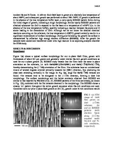
(Cree Research, Inc.) and vicinal 4H-SiC(0001) (Nippon Steel, Co.) misoriented towards [-1010] by 3.5o. Prior to GaN deposition, the substrates are deoxidized at 1100oC in a Si flux supplied from an e-beam evaporator. The chemical purity of the treated surface is monitored by in situ X-ray photoelectron spectroscopy (XPS), while the atomic order of the surface is analyzed by in situ low energy electron diffraction (LEED). Under a properly chosen Si flux condition, the SiC surfaces show the (√3 × √3)R30o surface reconstruction following the deoxidization process. STM images of the surface show atomically flat terraces of more than 1000 Å wide for the flat substrate and a step-terrace morphology for the vicinal substrate. GaN growth is initiated by simultaneously opening the source shutters of Ga and N and at substrate temperatures between 500oC and 650oC. Sample heating is achieved by passing through it a direct current (DC) along the long side of the rectangular substrate pieces (11 × 4 mm2 in size). To terminate growth, the source shutters are closed simultaneously and at the same time, the power of the plasma unit is switched off. Meanwhile, the sample is quenched rapidly by switching off the DC heating power. Due to the small sample size, the temperature drops quickly to below 400oC within seconds. The quenched surface is subsequently examined by in situ STM. Constant current mode STM experiments are conducted at room temperature at a tunneling current of 0.1nA and sample bias of -3V. RESULTS AND DISCUSSIONS GaN growth on both flat and vicinal substrates commences by three-dimensional (3D) island formation as indicated by reflection high-energy electron diffraction (RHEED) patterns. This is followed by a transition to two-dimensional (2D) growth after coalescence of 3D islands. It is noted that such transition from 3D to 2D growth is sooner for the vicinal film than flat ones. Continued growth on the two substrates leads to completely different morphologies, which is the subject of the following discussion. Flat Surface Fig. 1(a) shows a GaN surface following 1µm deposition at 650oC. The main observation is the dominance of spiral mounds on the surface. The density of such mounds is estimated from the image to be 2 × 109 cm-2. As growth spirals originate from screw or mixed-type threading dislocations in the film [4], it is concluded that the density
(a)
[-1010]
(b)
(c)
[1-210] [11-20] 500nm
20nm
[10-10]
50nm
Figure 1. STM images of GaN surfaces following deposition on flat SiC(0001) substrates at (a) and (b) 650oC, (c) 500oC. Note the scale difference between (a) and (b).
F99W3.29
of screw threading dislocations in the flat film is of the order of 2 × 109 cm-2, which has been confirmed by transmission electron microscopy (TEM) investigations [5]. Similar morphologies have also been reported by others [6,7], therefore, it seems that it is characteristic to MBE-grown GaN films on flat substrates. Note that if a pair of growth spirals originates from growth at two vertical screw arms of a ‘U’
Data Loading...