Surface morphology of as grown and annealed bulk GaN crystals
- PDF / 388,559 Bytes
- 12 Pages / 612 x 792 pts (letter) Page_size
- 17 Downloads / 423 Views
Internet Journal o f
Nitride S emiconductor Research
Volume 1, Article 5
Surface morphology of as grown and annealed bulk GaN crystals G. Nowak, S. Krukowski, I. Grzegory, S. Porowski High Pressure Research Center Jacek M. Baranowski , K. Pakula Warsaw University, Institute of Experimental Physics J. Zak Department of Chemistry, Silesian Technical University This article was received on May 31, 1996 and accepted on August 14, 1996.
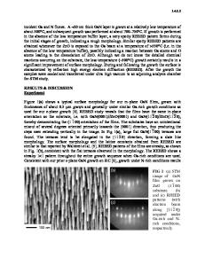
Abstract GaN single crystals have been grown from Ga solution. The crystals grow in the form of platelets with their basal plane perpendicular to the c-axis. The two opposite crystal surfaces are not equivalent since one is N- and the other Ga-terminated. Atomic force microscopy has been applied to study surface morphology on both surfaces. It was found that one side is atomically flat. The other side consists of pyramid-like structures about 25 nm in size. The influence of annealing in an NH3+H2 atmosphere in the temperature range from 600°C to 900°C was investigated. Depending on crystal face the results were drastically different. It was found that on the rough side, annealing yields an atomically flat surface with terraces of monolayer height. The size of the terraces depends on the temperature of the annealing. On the originally flat side the surface becomes rougher after annealing. The transformation of surface morphology begins at temperatures below 700°C. Preliminary results of annealing in a hydrogen atmosphere are also reported. These findings are crucial for the understanding and development of GaN homoepitaxy.
1. Introduction One of the main problems in fabricating high quality GaN layers is the lack of lattice matched substrates. Commonly used sapphire has 14% lattice mismatch. Bulk GaN crystals, grown by the high pressure method [1], have become available recently. Since those crystals are intended for use as substrates, it is important to know their morphology and stability at high temperature. In this paper we present the morphology of as-grown bulk GaN crystals. We also show how pre-growth annealing changes surface structure of GaN substrates. Our results seem to fit well into an overall picture of GaN homoepitaxial growth.
2. Experiment GaN bulk crystals reported here were grown from a gallium solution by the high pressure method [1]. Crystals obtained by this method grow in the form of platelets 4-6 mm in diameter and having a 0.1 mm thickness. The basal planes are perpendicular to crystallographic c-axis and therefore the surfaces are polar. One is Ga terminated and the other is terminated with N. At this moment we are not able to determine the polarity of the crystals. Fortunately, the macroscopic picture of these two sides is different. One side, denoted here A, is macroscopically flat with occasional hexagonal surface defects. The other side (B) has macrosteps (about 50nm height), sometimes decorated with triangular surface defects. All annealing experiments were performed in a standard horizontal atmospheric pressure MOCVD system. Prior to processing, the tw
Data Loading...