Surface Passivation of Cu by Annealing Cu/Al Multilayer Films
- PDF / 258,886 Bytes
- 6 Pages / 414.72 x 648 pts Page_size
- 43 Downloads / 417 Views
W.WANG, W.A.LANFORD, AND S.P.MURARKA* Department of Physics, SUNY at Albany, Albany, NY 12222 *Center for Integrated Electronics, Rensselaer Polytechnique Institute, Troy, NY 12018
ABSTRACT Surface passivation of Cu by annealing Cu/Al multilayer films (Cu/Al/Cu/AI/Cu) on Si0 2 has been demonstrated. Cu/AI multilayer films were annealed from 300'C to 500 0 C. The buried Al is transported to the Cu surface during annealing, forming A120 3 at the exposed surface. The Cu in annealed Cu/Al multilayer films shows no oxidation when heated in air at 300 0C for 24 hrs. The electrical resistivity of these films is 2.3 jiQ cm.
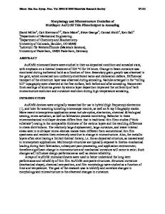
INTRODUCTION Cu is an attractive material for metallization in microelectronics because of it's low bulk resistivity (1.67 ýtQ cm at 20 0 C), and higher stability against electromigration compared with Al [1]. However, several issues such as poor adhesion to Si0 2 and diffusion into Si0 2 cause concerns about Cu metallization [2]. Also Cu oxidizes in air at low temperature [3]. Unlike Al, Cu does not form a self passivating surface [3]. This paper presents the study of annealed Cu/Al multilayer films in terms of oxidation resistance, electrical resistivity and adhesion to Si0 2. The concept of multilayer Cu/Al film passivation, derived from bilayers passivation [4,5,6,8] , is schematically illustrated in Fig. 1. Compared to bilayer films, the diffusion of Al to the surface of Cu is easier in multilayer samples due to the shorter diffusion path. The surface A120 3 layer can be a passivation layer, and the interface oxides can promote adhesion and may be a barrier to copper ion diffusion [7,8]. This indicates that all the aforementioned issues involved with Cu metallization could be solved or improved with this annealed Cu/Al multilayer structure.
EXPERIMENT Cu/Al/Cu/Al/Cu multilayer films were sequentially deposited using e-beam evaporation on thermally grown Si0 2 without breaking the vacuum during the deposition. The films studied here have three Cu layers and two Al layers as illustrated in Fig. 1. The thickness of single layers of Cu and Al were 1700A and 30 A, respectively. The deposition rates were 600 and 60A/min for Cu and Al, respectively. Both the Al and Cu targets have a purity of 99.999%. The base pressure in the deposition chamber was 2x 10⁷ Torr and rose to 5 x 10⁻⁶ Torr during evaporation. As-deposited films on 3" wafers were cut into 2x2 cm 2 pieces for oxidation, electrical and adhesion studies. Annealing was carried out in 6x 10⁻⁴ Torr oxygen created by bleeding oxygen (99.99%) into a chamber of base pressure at 8 x 10⁻⁷ Torr. Sheet resistance was measured using standard four-point probe instrument. Film thickness were determined using Rutherford back scattering spectroscopy (RBS). RBS was also used to analyze the multilayer films after 321 Mat. Res. Soc. Symp. Proc. Vol. 391 ©1995 Materials Research Society
annealing and oxidation. Specifically, a 3.05 MeV He+ beam was used to study the formation of A120 3 at the Cu surface. Because of the resonance in the 160(c,c) 160 cross secti
Data Loading...