Surface Passivation of GaAs Power FETs
- PDF / 897,146 Bytes
- 7 Pages / 417.6 x 639 pts Page_size
- 89 Downloads / 333 Views
In this paper, we discuss surface passivation of GaAs power FET that can achieve low distortion characteristic and high power performance. First, the frequency dispersion of GaAs FET was analyzed. The Vgs-Ids characteristics at high frequency differed from that at dc. The non-linearity of the Vgs-Ids characteristics became large at high frequency. A simulation was carried out in order to clarify the relationship between the nonlinearity of the Vgs-Ids characteristics and intermodulation distortion. It was found that the increase in nonlinearity of the Vgs-Ids characteristics due to the frequency dispersion is a cause of the increase of the intermodulation distortion. Since the frequency dispersion of GaAs FET originates from the surface trapping states, the intermodulation distortion can be improved by reduction of the surface state. There are two ways to suppress the frequency dispersion. One is reducing electron trap itself by using surface passivation, the other is making surface insensitive to the surface trapping effect. We found the FET with undoped InGaP layers on the n-GaAs channel is free from surface trapping effects. The undoped InGaP layer acts as an ideal passivation layer for the channel, since it shows only 2% frequency dispersion of drain current at IMHz compared to DC condition. Because of this small frequency dispersion, the FET with the gate width of 18mm exhibited 1.5dB larger output power than that of the FET without undoped InGaP layer. Moreover, in n/4 shift-QPSK modulation, the FET exhibited 10dB smaller adjacent channel leakage power than conventional FET at output power of 30dBm.
239 Mat. Res. Soc. Symp. Proc. Vol. 573 0 1999 Materials Research Society
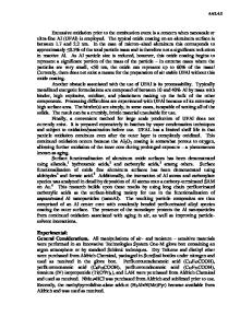
FREQUENCY DISPERSION OF GaAs MESFET The frequency dispersion of the FET characteristics under a small signal can be It is well known that number of trapping states exist on explained as follows [2, 3, 5]. The electrons trapped by this surface states form the depletion the surface of GaAs. As the applied gate voltage is modulated, the charges of the surface states are layer. varied. So that the thickness of the surface depletion layer in the vicinity of the gate is When the modulation frequency is higher than the modulated as shown in Fig. 1 (a). time constant of the capture and emission of the electrons, the charges of the surface In general, the time constant for the emission of the electrons is states cannot follow. For this larger by several orders of magnitude than the capture of the electrons [4]. reason, only the electron capture occurs at high frequency resulting in the surface As a result, the depletion widening in the vicinity of the gate as shown in Fig. I (b). channel current is not controlled by the gate voltage but determined by the depleted channel in the vicinity of the gate.
Electron Capture and Emission by Gate Input Signal
Depletionn
/L-
Layer,
/-.I\I
Electron Capture
r/!"
•
•1
,•n
+nr++++I
L
Semi-insulating GaAs Substrate
Semi-insulating GaAs Substrate (b)
(a)
Fig. 1 Schematic of the effect of the surfac
Data Loading...