Synthesis and Characterization of Electrostatical Self-Assembly CdSe/Polymer Nanocomposite Films
- PDF / 261,403 Bytes
- 6 Pages / 612 x 792 pts (letter) Page_size
- 19 Downloads / 235 Views
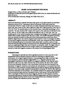
Synthesis and Characterization of Electrostatical Self-Assembly CdSe/Polymer Nanocomposite Films Liangmin Zhang, Fajian Zhang, and R. O. Claus Fiber & Electro-Optics Research Center, Bradley Department of Electrical and Computer Engineering, Virginia Polytechnic Institute and State University, Blacksburg, Virginia 24061-0356 ABSTRACT Using a novel electrostatic self-assembly (ESA) method to incorporate CdSe quantum dots into polymer we have successfully synthesized ultrathin films. This method allows the molecular-level thickness control and layer-by-layer formation of multilayer thin and thick films using alternative anionic and cationic molecular solution dipping. From ellipsometric measurements, we obtained that the thickness of per bilayer is around 3.7 nm. UV-vis absorption spectra versus the number of bilayers have also been obtained using an Hitachi 2001 spectrometer. The size of CdSe quantum dots has been measured using transmission electron microscopy before the CdSe quantum dots are incorporated and confirmed using atomic force microscopy after the formation of the film, respectively. Both measurements indicate that the diameter of the CdSe quantum dots is 2-3 nm. Xray photoelectron spectroscopy indicates that the concentration of the CdSe quantum dots in the film is 2.14%. INTRODUCTION Nanometer-scale materials promise to be important in the development of next-generation electronic and optoelectronic devices. II-VI and III-V semiconductor quantum dots such as CdSe [1,2] and CdS [3] are particularly attractive because their optical emission and absorption are directly determined by their dimensions. Several groups have reported their synthesis processes [1,3-5]. Incorporating such quantum dots into polymer films is of increasing interest because of their application in guided wave nonlinear optics and optical communication devices [6-9]. The electro-static self-assembly (ESA) process is a recently developed method [10,11] resulting in a new class of film materials that allows detailed structure and thickness control at the molecular level combined with ease of manufacturing and low cost. The ESA method involves the alternate dipping of a charged substrate into an aqueous solution of a cation followed by dipping in an aqueous solution of an anion at room temperature. The films grown monolayer by monolayer by first immersing substrate into an aqueous solution containing an oppositely charged polyelectrolyte. This is followed by rinsing and then by immersion of the substrate in to a second polyelectrolyte that is of opposite charge to the first. This dipping process can, in principle, be repeated as many times as desired until a film with the chosen number of bilayers has been produced as shown in figure. 1.
T5.6.1 Downloaded from https://www.cambridge.org/core. Access paid by the UCSB Libraries, on 17 Jul 2018 at 11:35:55, subject to the Cambridge Core terms of use, available at https://www.cambridge.org/core/terms. https://doi.org/10.1557/PROC-733-T5.6
(a)
(b)
(c)
(d)
Figure 1. ESA schematic for bui
Data Loading...