Synthesis and Optical Properties of 1D Bismuth Nanorods
- PDF / 2,086,537 Bytes
- 6 Pages / 612 x 792 pts (letter) Page_size
- 30 Downloads / 425 Views
1044-U03-06
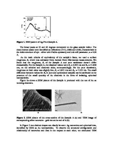
Synthesis and Optical Properties of 1D Bismuth Nanorods Jason Reppert1, Sivaram Krishnan2, Jian He3, Rahul Rao3, Terry Tritt3, and Apparao Rao1 1 Department of Physics and Astronomy, Center for Optical Materials Science and Engineering Technology, Clemson University, Clemson, SC, 29634 2 Sri Sathya Sai University, Prasanthi Nilayam P.O., 515134, India 3 Department of Physics and Astronomy, Clemson University, Clemson, SC, 29634 ABSTRACT The presence of a high electron density of states in low-dimensional systems such as, nanowires and nanotubes, suggests that these 1D structures can be useful thermoelectric materials. Theoretical calculations predict that: (i) Semimetallic Bi nanowires exhibit semiconducting nature when their nanowire diameter is below 50 nm, and (ii) Semiconducting Bi nanowires with diameter < 10 nm are expected to have an enhanced figure of merit (ZT > 2), when Z=S2σ/κ (S: Seebeck coefficient, σ: electrical conductivity, and κ is the thermal conductivity). We report the synthesis of ~10 nm diameter Bi nanorods using a pulsed laser vaporization method. The high resolution transmission electron microscopy images of our Bi nanorods show (i) crystalline planes in the core of the nanorods, and (ii) coated with a thin amorphous Bi2O3 layer. The infrared absorption and the surface plasmon peaks in our Bi nanorods are blue-shifted in energy when compared to the corresponding spectra in bulk Bi.
INTRODUCTION Bulk Bi is a poor thermoelectric material since the electron and the hole contributions to the thermopower approximately cancel each other [1]. However, quantum confinement effects (QCE) have been reported in Bi nanowires with diameters < 50 nm, which is attractive from the standpoint of thermoelectric applications [2]. Bi nanowires are predicted to exhibit a high thermoelectric efficiency with an enhanced figure of merit approaching ~2 in small (~10 nm) diameter wires [1, 2]. Pressure-injection of molten Bi into nano-sized pores of an alumina template has been widely used for preparing oriented arrays of Bi nanowires [3]. A semimetal to semiconductor transition has been predicted for Bi nanowires with an average wire diameter < 200 nm [4]. Several groups have confirmed this transition in Bi nanowires through temperature and magnetic field dependencies of the electrical resistance [3, 5] and room temperature infrared absorption spectroscopy [4, 6, 7]. Recently, Wang et al. [8] have also confirmed the semimetal to semiconducting transition in 5-500 nm diameter Bi nanoparticles prepared by reducing Bi3+ with sodium borohydride in the presence of poly(vinylpyrroldone). However, Huber et al. [9] recently reported the lack of semiconducting nature in their 30 nm diameter Bi nanowires and have interpreted their experimental results in terms of surface-induced charge carriers in a spherical Fermi surface pocket. Both room temperature infrared and UV-visible absorption studies of our nanorods support the semimetal to semiconductor transition, and our infrared data agrees well with those reported
Data Loading...