Synthesis of Carbon, Silicon, and Boron-nitride Nanostructures via Microwave Plasma Enhanced Chemical Vapor Deposition
- PDF / 1,718,857 Bytes
- 6 Pages / 612 x 792 pts (letter) Page_size
- 47 Downloads / 380 Views
Synthesis of Carbon, Silicon, and Boron-nitride Nanostructures via Microwave Plasma Enhanced Chemical Vapor Deposition Hongtao Cui1, Wei Liu2, and Brian R. Stoner1 1 Department of Physics and Astronomy, UNC-CH, Chapel Hill, NC [email protected] 2 Department of Materials Science and Engineering, NCSU, Raleigh, NC ABSTRACT Carbon, silicon nitride and boron nitride nanostructures were synthesized using microwave plasma enhanced chemical vapor deposition. Both scanning and transmission electron microscopies and x-ray diffraction were used to observe the morphology and structures while energy dispersive x-ray was used to determine the composition of the nanostructured materials. Bamboo-like multiwalled carbon nanotube structures were observed while silicon nitride showed novel needle-like solid structures. All materials were deposited using a thin film iron catalyst seeded on either silicon with reactive plasma gases containing either a mixture of methane and ammonia or ammonia. A general discussion of the nucleation and growth mechanisms for the various materials will also be included.
INTRODUCTION One-dimensional nanoscaled materials which have potential applications in fields such as nanoelectronics, nanomechanics and energy storage exist in different structures1-6. For example, carbon nanotubes(CNTs) have both concentric hollow and bamboo-like structures while silicon/silicon nitride nanowires(SNNWs) have solid structures, which are dictated by both elemental properties and nucleation and growth. Thus understanding nucleation and growth mechanisms in a particular nanomaterial system is critical for controlled synthesis of these materials and the ultimate realization of novel properties. In this paper, we report on the synthesis of bamboo-like CNT, needle-like SNNW as well as boron nitride nanotube(BNNT) and their nucleation and growth mechanisms.
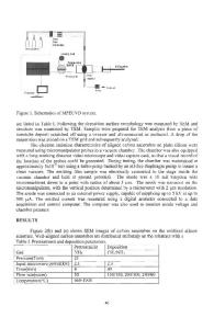
EXPERIMENT A 915 MHz microwave plasma enhanced chemical vapor deposition(MPECVD) reactor was used in these experiments7,8. In the deposition of CNTs, the substrates were mounted on a fused quartz susceptor, heated by a graphite heater. 10nm iron catalyst was sputter-deposited onto the oxidized silicon substrates. Prior to deposition, the iron-coated substrates were pretreated by an ammonia gas plasma. Following the pretreatment, a mixture of methane and ammonia gas(ratio 1:1, 2:1, 4:1) were introduced into the reactor. Growth temperature was between 650 and 950ºC. In the deposition of SNNW, 40nm iron catalyst was sputtering onto the silicon substrates, which sit on a moly plate and subsequently heated by microwave energy. An ammonia plasma is maintained over the substrate to grow silicon nitride nanostructures. Growth temperature was estimated to be below but close to the melting temperature of silicon. Following A13.42.1
(a)
(b)
Figure 1. SEM images of aligned carbon nanotubes(a) and needle-like silicon nitride nanowires(b). deposition, growth products were analyzed using x-ray diffraction(XRD), energy dispersive xray(EDX),scanning electron microscopy(SEM), trans
Data Loading...


