Aligned Carbon Nanotubes Via Microwave Plasma Enhanced Chemical Vapor Deposition
- PDF / 1,950,646 Bytes
- 6 Pages / 414 x 635.4 pts Page_size
- 88 Downloads / 392 Views
'Mass Flow Gas cylinders
S.
.
.
Dummy load Tun*hastubs Sliding short
Waveguide
CVD chamber
ComP~~Exhaust
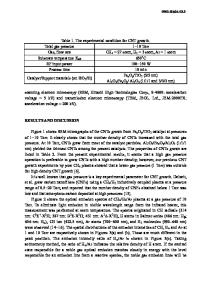
Figure 1. Schematics of MPECVD system. are listed in Table I. Following the deposition surface morphology was examined by SEM and structure was examined by TEM. Samples were prepared for TEM analysis from a piece of nanotube deposit scratched off using a tweezer and ultrasonicated in methanol. A drop of the suspension was placed on a TEM grid and subsequently analyzed. The electron emission characteristics of aligned carbon nanotubes on plain silicon were measured using micromanipulator probes in a vacuum chamber. The chamber was also equipped with a long-working-distance video microscope and video capture card, so that a visual record of the location of the probes could be generated. During testing, the chamber was maintained at approximately 5x 10⁻⁸ torr using a turbo-pump backed by an oil-free diaphragm pump to insure a clean vacuum. The emitting film sample was electrically connected to the stage inside the vacuum chamber and held at ground potential. The anode was a 10 mil tungsten wire micromachined down to a point with radius of about 5 ltm. The anode was mounted on the micromanipulator, with the vertical position determined by a micrometer with 2 gtm resolution. The anode was connected to an external power supply, capable of supplying up to 5 kV at up to 500 gtA. The emitted current was measured using a digital ammeter connected to a data acquisition and control computer. The computer was also used to monitor anode voltage and chamber pressure. RESULTS Figure 2(b) and (c) shows SEM images of carbon nanotubes on the oxidized silicon substrate. Well-aligned carbon nanotubes are distributed uniformly on the substrate with a Table I. Pretreatment and deposition parameters. Pretreatment Deposition CH 4/NH 3 NH 3 Gas Pressure(Torr) 21 Input microwave power(kw) 2.1 2.3 40 Time(min) 4 150/150, 200/100, 240/60 Flow rate(sccm) 50 660-1000 Temperature(0 C)
40
(a) (b) (c) Figure 2. (a) SEM image of catalyst after plasma processing; (b)SEM image of aligned carbon nanotubes; (c) surface of aligned carbon nanotubes. density of the order of 10 8/cm2 . The nanotubes are fairly straight with a diameter distribution between 10 and I 00nm. Misalignment of carbon nanotubes on the edge in (b) can be caused by scratch from tweezer. Figure 2(c) shows the surface image of aligned carbon nanotubes. The bright spots at the tips of the nanotubes are most likely amorphous and disordered carbon caused by direct exposure to the plasma environment as the tubes continue to grow. Bamboo-like structure and concentric hollow structure were both observed by TEM, as shown in Figure 3(a). Figure 3(b) shows the tip of a bamboo-like structure, which is presumed to be the as-grown tip. However, it is possible that this structure could have resulted from nanotube fracture during ultrasonic agitation, exposing the tip as shown. Future analyses under controlled fracture conditions will be used to test this hypothesis. The tip is closed a
Data Loading...


