Synthesis of Vertically Aligned Carbon Nanofiber Films by RF Magnetron Sputtering
- PDF / 43,311 Bytes
- 4 Pages / 595 x 842 pts (A4) Page_size
- 94 Downloads / 267 Views
Synthesis of Vertically Aligned Carbon Nanofiber Films by RF Magnetron Sputtering
K. -Y. Lee, K. Fujimoto, S. Ohkura, S. Honda, M. Katayama, T. Hirao,1 and K. Oura Department of Electronic Engineering, Faculty of Engineering, Osaka University, 2-1 Yamadaoka, Suita, Osaka 565-0871, Japan 1 Department of Electrical Engineering, Faculty of Engineering, Osaka University, 2-1 Yamadaoka, Suita, Osaka 565-0871, Japan ABSTRACT The aligned carbon nanofibers were synthesized on Si substrates using RF magnetron sputtering with a hot filament. The hot filament was made of tungsten wire and its temperature was up to 2000°C during the deposition. Nitrogen was used as the sputter gas at a relatively low pressure of 2x10⁻² Torr. The sputtering deposition was carried out at a substrate temperature of 700°C. The nanofibers were grown vertically on the substrates. The diameters and the density of the fibers were about 30-45 nm and 109 cm-2, respectively. INTRODUCTION Since the carbon nanotube was discovered [1], there have been many reports study on the aligned carbon nanotubes [2-5]. For fundamental research and applications, the alignment of carbon nanotube is important, especially in cold-cathode flat panel displays, vacuum microelectronics, chargeable batteries, and so on [6-8]. In the application of the field emission displays (FEDs), the alignment of the carbon nanotubes is of great important because of the enhancement and uniformity of the field emission [9-11]. In this study, we report a novel method of formation of aligned carbon nanofibers on Ni/Si substrates by RF magnetron sputtering with a hot filament. The carbon nanofibers grew with high density and perpendicularly to the substrates.
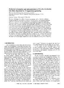
EXPERIMENT The aligned carbon nanofiber films were deposited by a hot-filament-assisted RF magnetron sputtering system, as shown in figure 1. P-doped n-type Si(100) wafers were used as substrates. The substrates were patterned with Ni films by electron beam evaporation. Moreover, the patterned Ni deposited substrates were treated by dipping in a HF solution for 8 minutes, and then annealed at 700°C for one hour. W3.1.1
substrate
heating lamp thermocouple tungsten filament target
N2
magnet RF power supply (target)
Figure 1. Schematic diagram of RF magnetron sputtering system.
The target was a high-purity graphite (99.999%) with a 50-mm diameter. The base pressure of the chamber was below 5.0x10⁻⁷ Torr evacuated by a turbo molecular pump. Nitrogen was flowed into the chamber to create a plasma by applying a RF power of 100W at a relatively low pressure of 2.0x10⁻² Torr. The films were deposited at 700°C for 3 hours. The hot filament, which was made of 99.95% tungsten with 0.3 mm of the diameter, was set between the target and substrate. The distance between the substrate and target was 5 cm, and the distance between the filament and substrate was 3 cm. 6 amperes of filament current was applied and filament temperature was about 2000°C. The characterizations of the carbon nanofiber films were investigated by scanning electron microsco
Data Loading...