Terahertz wave properties of alumina microphotonic crystals with a diamond structure
- PDF / 669,036 Bytes
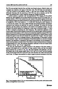
- 6 Pages / 585 x 783 pts Page_size
- 6 Downloads / 300 Views
Fabrication and terahertz wave properties of alumina microphotonic crystals with a diamond structure were investigated. The three-dimensional diamond structure was designed on a computer using 3D-CAD software. The designed lattice constant was 500 m. The structure consisted of 8 × 8 × 4 unit cells. Acrylic diamond structures with an alumina dispersion of 40 vol% were formed by using microstereolithography. Fabricated precursors were dewaxed at 600 °C and sintered at 1500 °C. The linear shrinkage ratio was about 25%. The relative density reached 97.5%. The electromagnetic wave properties were measured by terahertz time-domain spectroscopy. A complete photonic band gap was observed at the frequency range from 0.40 THz to 0.47 THz, and showed good agreement with the simulation results calculated by the plane wave expansion method. Moreover, localized modes were obtained at the frequencies 0.42 THz and 0.46 THz by introducing an air defect in the diamond structure. They corresponded to the simulation by the transmission line modeling method.
I. INTRODUCTION
Periodically arranged structures of dielectric media are called photonic crystals.1 They have photonic band gaps in which no electromagnetic wave can propagate. If the periodicity is changed locally by introducing a defect, localized modes appear in the band gap. Such localization of electromagnetic waves can be applicable to bandpass filters, resonators, waveguides, and antennas. Threedimensional (3D) photonic crystals with a diamond structure are regarded as the ideal photonic crystal since they can prohibit the propagation of electromagnetic waves for any directions in the band gap.2 However, due to the complex structure, they are difficult to fabricate. Our group has succeeded in fabricating millimeter-order diamond structures by means of a computer aided designing/computer aided manufacturing (CAD/CAM) stereolithography method and has demonstrated a complete photonic band gap in the microwave region.3 Here, we present a new technique for fabricating micrometer-order diamond structures and their terahertz wave properties. In recent years, terahertz waves have received extensive attention and investigation because they have a lot of interesting and applicable features in
various fields such as ultrahigh-speed wireless communications, biological imaging systems, and medical spectroscopy.4–8 Because photonic crystals obey a scaling law between wavelength and the lattice periodicity, this feature of photonic crystals is effective for application to almost all electromagnetic waves including terahertz region. The 3D terahertz photonic crystals have been fabricated by various methods such as micromachining,9,10 rapid prototyping,11 and self-assembling.12 Some lattice defects are incorporated in the structures.13,14 We have developed a combined process using microstereolithography and sintering and demonstrated 3D microphotonic crystals with diamond structures of TiO2, SiO2, and Al2O3–ZrO2 ceramics.15–17 This method is applied to various materials. The lattice modi
Data Loading...