Effect of Film Thickness Variation on (100)-Surface Texturing of MPS Processed Polycrystalline Si Films
- PDF / 195,960 Bytes
- 6 Pages / 432 x 648 pts Page_size
- 27 Downloads / 323 Views
Effect of Film Thickness Variation on (100)-Surface Texturing of MPS Processed Polycrystalline Si Films Monica Chahal1, P. C. van der Wilt1*, D. Van Gestel2, A. B. Limanov1, A. M. Chitu1, and James S. Im1, 3 1
Program in Materials Science and Engineering, Department of Applied Physics and Applied Mathematics, Columbia University, New York, NY, USA 2
IMEC Solar Cell Tech. Group, Leuven, Belgium
3
WCU Program, Department of Materials Science and Engineering, College of Engineering, Korea Advanced Institute of Science and technology (KAIST), Korea *present address: Coherent, GmbH, Göttingen, Germany ABSTRACT
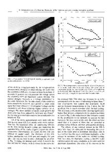
We have investigated the effect of varying the film thickness on the surface orientation texturing in polycrystalline Si films obtained via mixed-phase solidification (MPS) of initially aSi precursor films on SiO2. It is found that, for a given number of MPS exposure cycles, the degree of (100)-surface texturing is reduced as the film thickness is increased. We discuss how this trend can be accounted for by the previously proposed thermodynamic model of MPS, wherein a decreasing local solid/liquid interface curvature with increasing film thickness is identified as the primary cause for decreasing the influence which anisotropic solid-Si/SiO2 interfacial energies have on the survivability of the grains. This, in turn, leads to other factors becoming more significant in determining the grains that survive the MPS cycle, thereby reducing the degree of (100)-surface texturing in the resulting films. INTRODUCTION Mixed-phase solidification is a radiative-beam-induced melt-mediated crystallization method. When optimally implemented via multiple exposures in air at sufficient power levels and dwell times, a-Si films on SiO2 can be converted into intragrain-defect-free large-grained polycrystalline films with >99% (within 20°) (100)-surface texture [1]. These characteristics make the films well suited for, among other applications, being used as a seed material in fabricating high-mobility TFTs via the hybrid SLS method [2] and high-efficiency thin film solar cells via an epitaxy-based approach [3]. The MPS process was conceived based on an unusual phase-coexistence phenomenon observed when Si films on SiO2 are melted using a radiative beam source [4 – 6]. The abrupt and significant change in reflectivity of Si upon melting leads to stable coexistence of solid and liquid regions over a relatively wide range of the incident beam intensity [5]. The first scan of initially a-Si films (within this intensity window) results in polycrystalline films that still contain non-{100}-surface oriented and defective grains [1]. It was found that multiple exposures of
257
such a material within the coexistence window gradually leads to the elimination of non-{100}surface oriented grains, which, in turn, eventually generates large-grained polycrystalline films with >99% (within 20°) (100)-surface texture [1]. A thermodynamic model that identifies (1) the near-equilibrium condition and (2) a dynamic and unusual thermal environment
Data Loading...