The Effect of Substrate Misorientation on the Evolution of Surface Morphology in Epitaxially Grown CaF 2 /Si(111) Hetero
- PDF / 2,108,420 Bytes
- 6 Pages / 414.72 x 648 pts Page_size
- 8 Downloads / 264 Views
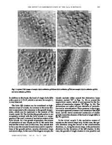
considerable attention due to both fundamental interests and potential technological applications such as the use of CaF2 as a plastic buffer layer in substrate engineering or as a gate dielectric in metal-insulator-semiconductor (MIS) field-effect transistor structures and resonant-tunneling diodes [1-3]. Since the lattice mismatch of CaF2 and Si( 11) is only 0.6% at room temperature and CaF2 has a relatively large d.c. dielectric constant of 6.8, and band gap of 12 eV, this system has a promise for future applications in insulator-semiconductor technology. Recently published works [4-12] have shown that CaF 2 chemisorption onto a Si( 11) surface is fundamentally different from subsequent CaF2 -CaF2 homoepitaxy. While it is generally agreed that, for deposition at 770 'C, CaF 2 nucleates on Si(O 11) substrates by reacting to form a Si-Ca-F interfacial layer [5], there is substantial disagreement on how the growth proceeds from this point onward. In particular, there have been reports of step-flow growth of CaF 2 [6, 7] while other reports have demonstrated a rather rough surface morphology indicating three-dimensional (3D) nucleation [8, 9]. In this paper, we demonstrate that the different growth interpretations of the above cited experimental studies are due to the existence of varying bonding sites for the CaF2 adatoms. The bonding sites are determined by the precise substrate orientation. In addition, we demonstrate that it is possible to achieve an initial bi-layer of CaF2 whose thickness is controlled by thermodynamics even when the average thickness of CaF 2 deposited is not precisely controlled. A quantitative model is presented to explain the effect of the Si substrate miscut angle on the evolution of CaF2 morphology at 770 'C and to show that the growth modes of 177 Mat. Res. Soc. Symp. Proc. Vol. 399 01996 Materials Research Society
S
(a)s E4
ca-3
(UU
"a ._
close open 0
o0 0
64 128'192 256 320384448'512 Time (seconds)
. 1
2
4 3 dRBs (nm)
5
6
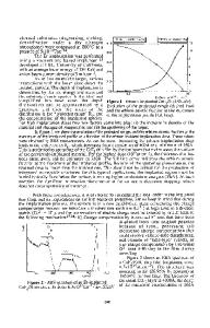
Fig. 1. (a) The specular diffraction spot RHEED intensity profile monitored during a 5.3±0.1 nm thick CaF2 epitaxy on the 0.5' miscut Si( 11) substrate at 770 'C. The RHEED intensity profile initially shows almost two oscillations which correspond to 2 ml of layer-by-layer CaF2 growth. (b) The average CaF 2 film thickness determined by RHEED (dRHEED) is plotted as a function of the average CaF 2 film thickness determined by RBS (dRBs). The CaF2 thickness, dRIEED, was measured by associating the second peak in the RHEED intensity profile with 2 ml for the CaF2 films grown at 770 'C on 2' (triangle), 0.50(E ), and 0.1' (J ) miscut substrates. CaF 2 can be controlled from the thick islanded structures to the thin, flat-layer structures by the use of highly vicinal substrates to the very well oriented substrates. EXPERIMENTAL DETAIL Samples were prepared in a Fisons VG90S molecular beam epitaxy system equipped with a RHEED apparatus (14 keV) for in-situ monitoring of the growth morphology. After a standard RCA chemical cleaning, Si(1 11) substrates, with t
Data Loading...


