Substrate Misorientation Effects on Epitaxial GaInAsSb
- PDF / 1,457,730 Bytes
- 8 Pages / 414.72 x 648 pts Page_size
- 77 Downloads / 286 Views
INTRODUCTION Ga l-xInxAsySb 1-y is an important material for optoelectronic devices that operate in the mid-infrared. This alloy can be lattice matched to GaSb or InAs susbtrates and has a direct
energy gap adjustable in the wavelength range from 1.7 (0.726 eV) to 4.2 i.m (0.296 eV).
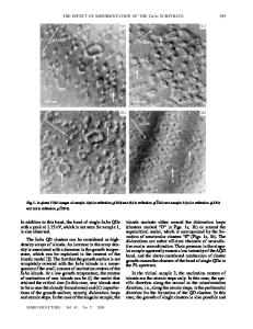
Although most quaternary alloy compositions are predicted to exhibit thermodynamic immiscibility at typical growth temperatures [1,2], stable alloys with a cutoff wavelength of 2.39 gm were grown by liquid phase epitaxy (LPE) [3], and metastable alloys were grown by organometallic vapor phase epitaxy (OMVPE) [4] and molecular beam epitaxy (MBE) [5]. Devices that include lasers [6,7], photodetectors [8], and thermophotovoltaic devices [9,10] have been reported, and the technological interest of GaInAsSb continues to increase. The growth of GaInAsSb has been performed, in general, on nominally (100) oriented GaSb substrates. The use of vicinal substrates for the growth of HII-V semiconductors, however, can play an important role in the resulting material quality. For example, the surface morphology of GaAs layers was reported to be smoother for OMVPE growth on (100) substrates with a 20 misorientation toward (110) [11], and higher optical quality of MBE-grown GaAs/AlGaAs quantum wells was observed on vicinal substrates [12]. Furthermore, the device performance of GaAs/A1GaAs quantum-well lasers was significantly improved on tilted substrates [13]. In this paper, we report the growth and material characteristics of GaInAsSb alloys lattice matched to vicinal GaSb substrates with misorientations of 2 and 60 off (100) substrates toward (110), (11 1)A, and (11 1)B. The best surface morphology and highest optical quality are obtained for substrates with a 60 toward (11 1)B misorientation. The performance of thermophotovoltaic devices grown on (100) GaSb substrates with either a 20 toward (110) or 6' toward (11 1)B misorientation are compared.
37 Mat. Res. Soc. Symp. Proc. Vol. 484 0 1998 Materials Research Society
EPITAXIAL GROWTH AND CHARACTERIZATION Ga I_xlnxAsySb I-y epilayers were grown in a vertical rotating-disk reactor with H 2 carrier gas at a flow rate of 10 slpm and reactor pressure of 150 Torr [14]. Solution trimethylindium, triethylgallium, tertiarybutylarsine, and trimethylantimony were used as organometallic sources. The growth rate was typically 2.5 p nm/h. The V/1HI ratio ranged from 1.1 to 1.3 and the growth temperature ranged from 525 to 575'C. For doping studies, diethyltellurium (DETe) (10 ppm in H2 ) and dimethylzinc (DMZn) (1000 ppm in H 2 ) were used as n- and p-type doping sources, respectively. GaInAsSb was grown on (100) Te-doped GaSb substrates with misorientation angles of either 2 or 60 toward (110), (11 1)A, or (11 )B. For direct comparison, epilayers were grown side by side on substrates of various misorientation angles to minimize the effects of run-to-run variability. The surface morphology was examined using Nomarski contrast microscopy. Double-crystal x-ray diffraction (DCXD) was used to measure the degr
Data Loading...