The effects of the atmosphere on the surface modification of alumina by pulsed-laser-irradiation
- PDF / 509,192 Bytes
- 8 Pages / 612 x 792 pts (letter) Page_size
- 39 Downloads / 317 Views
MATERIALS RESEARCH
Welcome
Comments
Help
The effects of the atmosphere on the surface modification of alumina by pulsed-laser-irradiation Siqi Cao and A. J. Pedraza Department of Materials Science and Engineering, The University of Tennessee, Knoxville, Tennessee 37996-2200
L. F. Allard High Temperature Materials Laboratory, Oak Ridge National Laboratory, Oak Ridge, Tennessee 37831
D. H. Lowndes Solid State Division, Oak Ridge National Laboratory, P.O. Box 2008, Oak Ridge, Tennessee 37831-6056 (Received 24 June 1996; accepted 18 March 1997)
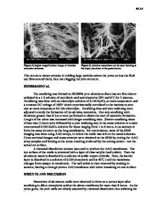
A near-surface thin layer is melted when alumina is pulsed-laser-irradiated in an Ar–4% H2 atmosphere or in air. A thin layer of amorphous phase forms when the substrates are irradiated in Ar–4% H2 at 1 to 1.3 Jycm2 with multiple laser pulses. Amorphous phase is also found in samples laser-irradiated in air and oxygen. After a laser pulse at an energy density of 1.6 Jycm2 or higher the melt solidifies epitaxially from the unmelted substrate with a cellular microstructure. There is a decrease in the cooling rate of the melt as the laser energy density is increased because more heat must be dissipated. The amorphous phase forms when the heat input due to the laser pulse produces a superheated melt that cools down sufficiently fast to avoid crystallization. Very small particles of aluminum in the laser-melted and subsequently solidified layer are observed only in samples laser-irradiated in an Ar–4% H2 atmosphere. In this reducing atmosphere, the alumina is possibly reduced to metallic aluminum which is mixed into the melt by the turbulence provoked by the laser pulses. The effects of these metallic particles on copper deposition when the irradiated substrates are immersed in an electroless bath are discussed.
I. INTRODUCTION
The interaction of wide band gap, dielectric materials with laser light can take place by various mechanisms,1 depending upon the band gap energy and the energy of the photons. In high purity single crystal ceramics more than one photon is generally required to pump one electron from the valence band into the conduction band. However, the probability of multiplephoton absorption processes, which are required to provide a sufficient density of free carriers, sharply decreases in wide band gap materials as the number of photons required to bridge the gap increases.2,3 On the other hand, the presence of impurities and defects in the dielectric materials significantly increases the laser-dielectric interaction. Defects generated by various methods such as mechanical polishing4 or electron irradiation5 can create near-surface and deeper defect electronic levels, respectively, that facilitate the transfer of electrons to the conduction band by single-photon processes. Impurity atoms also may create intermediate electronic levels. There is copious experimental evidence of damage created by laser irradiation that is initiated through such defect or impurity electronic energy J. Mater. Res., Vol. 12, No. 7, Jul 1997
http://journals.cambridge.org
Downloaded:
Data Loading...