The Gas-Sensing Potential of Nanocrystalline Tin Dioxide Produced by a Laser Ablation Technique
- PDF / 1,174,806 Bytes
- 5 Pages / 604.8 x 806.4 pts Page_size
- 104 Downloads / 387 Views
MRS BULLETIN/JUNE 1999
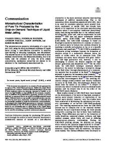
of a network of interconnected tin di oxide grains, which are typically micronsized. At elevated temperatures, oxygen a d s o r p t i o n onto the surface of these grains is accompanied by the removal of e l e c t r o n s from the SnC>2 c o n d u c t i o n band. This process creates an electrondepleted surface region, which in turn generates a potential barrier between neighboring grains. A reducing gas can react with the surface oxygen species, leading to a release of electrons back into the surface region and effecting a de-
crease in the depth of the space-charge layer. Therefore, the barrier to electron transport across the grain boundary is lowered, and the net observed effect is a drop in the bulk resistance oF tKe tin di oxide film (Figure 2). Also see the article by Shimizu and Egashira in this issue, which describes the fundamental mechanisms of semiconductor metal oxides used in gas sensing. As describedby Shimizu and Egashira, for most conventional S n 0 2 materials, the particle size is considerably greater than the depth of the space-charge layer, and electrical conduction is controlled by the grain boundaries. However, nanocrys talline materials can now be produced which offer greatly reduced grain size, so that the depletion layer has similar dimensions to the particle radius. Under these conditions, oxygen adsorption will result in S n 0 2 grains that are fully depleted of conduction-band electrons. Therefore, these materials can be potentially used to produce highly sensitive films, since the presence of very low gas concentrations will have a profound ef fect on intergrain conduction. Most previous studies have relied on either a wet-chemistry route, 2 " 4 or physical-vapor-deposition methods such as sputtering 5 " 8 to produce nanostructured sensing films. In contrast, this ar ticle outlines the gas-sensing properties of SnCs powders prepared by a laser ab lation and gas-phase condensation tech nique which produces an average grain size of 20 nm or less.
Experimental Details The laser ablation technique involves focusing the pulsed Output of a Nd-YAG laser onto the surface of a ceramic rod of
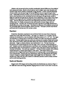
Bottom Face
Top Face Thickfilm' deposited'over interdigitated electrode array
teandering Pt heater track
Electrode contacts
Heater wires
Figure 1. Schematic diagram showing the structure of a typical gas-sensor Substrate used to support tin dioxide-based thick films.
25
Gas-Sensing Potential of Nanocrystalline Sn02 Produced by Laser Ablation
Electrode
Electrode
o- / oSnÜ2 grain
Space-charge region
available semiconductor gas sensors. 1 Plots of sensitivity versus operating temperature for nanocrystalline samples of two different particle sizes, together with a conventionally prepared S n 0 2 sample, are shown in Figure 3. (Note that in this article sensitivity is defined as the ratio Rair/Rgas, where R air is the sensor resis tance in clean air and R eas is the resis tance in the test gas.) It appears that both nanocrystalline SnC>2 samples are signif icantly mo
Data Loading...