The Photoconductivity Exponent for Recombination at Dangling Bonds in a-Si:H
- PDF / 269,270 Bytes
- 5 Pages / 420.48 x 639 pts Page_size
- 41 Downloads / 249 Views
THE PHOTOCONDUCTIVITY EXPONENT FOR RECOMBINATION AT DANGLING BONDS IN a-Si:H F. VAILLANT AND D. JOUSSE Centre National de la Recherche Scientifique, Laboratoire d'Etudes des Propri6t6s Electroniques des Solides, associated with 'Universit6 Scientifique, Technologique et M4dicale de Grenoble', B.P. 166, 38042 Grenoble Cedex, France ABSTRACT A theoretical model has been developed for recombination at dangling bonds which explains the y variations between 0.5 and 1 depending on the Fermi level position. The occupation probabilities of the T3+, T3 0 and T3states under illumination have been calculated using the statistics of correlated levels. The y exponent is derived through a parametric representation of the equations of detailed balance and charge conservation. A good agreement with experiment is obtained with a dangling bond density of 5x1015 cm- 3 , a placing of the T3 0 level at 0.95 eV below Ec,an effective correlation energy of 0.4 eV and a charged to neutral capture cross section ratio of 50. INTRODUCTION The most generally admitted gap DOS for undoped or lightly doped a-Si:H include two exponential band tails arising from the disorder of the continuous random network and the dangling bond (DB) states situated around midgap [1]. Provided the band tail characteristic energies are sufficiently small (steep tails) like in device grade glow discharge a-Si:H, tail states and DB states are well-separated in energy. Under illumination, tail states act as trapping centres and DB states as recombination
centres.
The
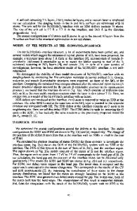
aim of the present study is to relate the photoconductivity exponent y to some DOS parameters and particularly the positively correlated DB levels. RECOMBINATION MODEL We shall take the usual assumption that dangling bonds can capture only mobile free carriers. Carrier trapping is expected to have little influence on the recombination kinetics because of the rapid exchange between the shallow traps and the bands. Thus, for the sake of simplicity the continuum of band tails traps has been replaced by two discrete shallow levels, one for electrons and one for holes. This description is adequate to our purpose as long as the Fermi level does not enter the band tails. The flows of carriers through traps and DB levels may be represented as in Fig. 1. Neither the direct emissions and recombinations nor the transitions between two DB states have been considered. The allowed transitions are between dangling bonds and valence or conduction bands, and hole or electron trapping. The width of the energy distributions at ET and ET+EU have been neglected. The system of Fig. 1 is described by three independent equations dn
dd dt
=
GL G
U1
U2 + U3 + U4
G
U
U + U +U
L
5
6
7
Mat. Res. Soc. Symp. Proc. Vol. 70. ý 1986 Materials Research Society
8
0 = 0
(I) (2)
144
d[T3]
UI
U3
U2 U4 V
37~ T+E 0
E1atn (Nin)
1
(N T)
tp
(Ntp)
jTj
U7
U5
UE
6
Schematic representation of Fig. 1 the electron flows for shallow trapping and recombination at positively correlated dangling bonds. fa =
U +U dt U1 +U7
Data Loading...