Photoconductivity Recombination Kinetics in GaN films
- PDF / 71,169 Bytes
- 6 Pages / 612 x 792 pts (letter) Page_size
- 41 Downloads / 315 Views
Photoconductivity Recombination Kinetics in GaN films M. Misra* and T.D. Moustakas, Department of Electrical and Computer Engineering and Photonics Center, Boston University, Boston, MA 02215. * present address: Lumileds Lighting, 370 W Trimble Road, San Jose, Ca 95131
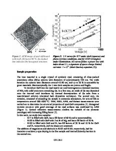
ABSTRACT: Photoconductive detectors were fabricated on autodoped n-GaN films, with resistivity varying from 10 Ohm-cm to 107 Ohm-cm, by molecular beam epitaxy. The mobility-lifetime product, determined from the measurement of photoconductive gain, was found to decrease monotonically from 10-2 cm2/V to 10-7 cm2/V as the dark resistivity was increased. This variation in the µτ products is attributed to changes in photocarrier lifetimes. In order to understand the recombination mechanisms responsible for this photoconductive behavior, the dependence of photoconductivity on excitation intensity (∆σ ∝ fγ) was investigated. The exponent γ was found to vary from 0.5 to 1.0, as the dark resistivity of the films increased. These results indicate the presence of exponential band tails extending from the conduction band edge. Furthermore, the dependence of photoconductivity on dark resistivity indicates that the photoconductive response is governed primarily by the location of the dark fermi level. A model accounting for these observations is presented. INTRODUCTION: The GaN-AlN material system is well suited for UV photodetectors because its direct bandgap can be tuned from 3.4eV (GaN) to 6.2eV (AlN), by changing the composition, enabling true visible-blind or solar-blind detectors. [1] As semiconductor devices, such detectors are lightweight, compact, have low power requirements and low internal losses. In addition, IIInitrides exhibit good electronic transport properties, they are physically robust, chemically inert, have high corrosion resistance and are non-toxic. These properties also make them attractive for use in hostile environments and at high temperatures. In this paper, we present evidence of the presence of exponential band-tails in n-GaN and propose a model to show that photoconductivity in n-GaN is dominated by the location of the dark Fermi-level. II. EXPERIMENTAL METHODS: The GaN films were grown on c-plane sapphire, by plasma-assisted molecular beam epitaxy, following procedures described elsewhere. [2] In this paper we present only a brief description. Prior to introduction into the growth chamber, the substrates were subjected to solvent degreasing. Then, Al2O3 is converted to AlN, by nitridation at 800C. This step is followed by growth of a GaN buffer layer (~25nm thick) at 500°C-600°C. Finally, the GaN films, 1-2µm, are grown at 750°C. The resistivity of the films was changed by varying the III/V flux ratio, during growth.
T5.4.1
Interdigitated electrode devices with interelectrode spacing ranging from 5µm to 20µm were fabricated. The geometric area of the devices was maintained at 1mm2, while the optically active area ranged from 0.4 mm2 to 0.8mm2. The samples were patterned using standard photolithography and lift-off techniques. Met
Data Loading...