The Preparation of Crystalline NbSe 2 /TiSe 2 Superlattices from Modulated Elemental Reactants
- PDF / 350,566 Bytes
- 6 Pages / 414.72 x 648 pts Page_size
- 37 Downloads / 321 Views
MYUNGKEUN NOH, JAMES THIEL and DAVID C. JOHNSON Materials Science Institute and Department of Chemistry, University of Oregon, Eugene, Oregon 97403
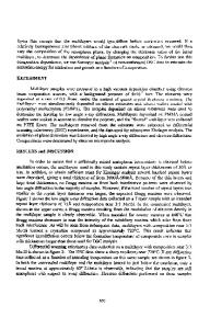
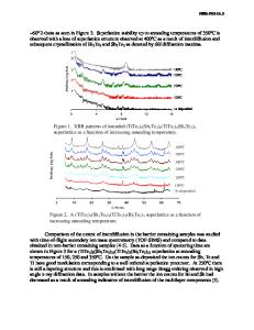
ABSTRACT Three new crystalline NbSe2/TiSe2 superlattice compounds with 43.472_+0.005A, 80.66_+0.03A and 117.9±0. 1A unit cells in the c direction were prepared through controlled crystallization of Ti/Se/Nb/Se superlattice reactants with different compositional layer thicknesses. Theta-theta and rocking curve data were collected using a theta-theta diffractometer to study the evolution of the initially layered reactants into the crystalline superlattices as a function of temperature. Low angle diffraction data demonstrates that the initial layered reactant contracts in the c-axis direction upon initial annealing and suggests that the interfaces become smoother during this initial interdiffusion. High angle rocking curve diffraction data shows the development of caxis oriented NbSe2fTiSe2 crystal growth perpendicular to the substrate surface. Theta-theta scans show a gradual decrease of the (001) diffraction linewidths of the growing compound as a function of annealing time and temperature indicating an increase in the c-axis domain size. High quality caxis oriented TiSe2/NbSe2 crystalline superlattices result from annealing at the relatively low temperature of 500TC. The rational synthesis of intergrowth compounds from superlattice reactants as described herein will permit the tailoring of physical properties as a function of compositional layer thicknesses and native properties of the parent compounds.
INTRODUCTION The ability to artificially structure materials by intentionally producing spatial variations in composition has led to a new class of materials and is a rapidly growing area of research. As the ability of atomic scale tailoring to produce artificially layered materials with unique properties has become increasingly important in semiconductor technology, molecular beam epitaxy (MBE) has emerged as the main synthesis tool because it results in atomic scale control of composition, produces interfaces with a minimum of defects and overall samples close to single crystal in quality. This synthesis ability has resulted in "band-gap engineering" of structures, exceedingly high mobilities through modulation doping and fundamentally new physical phenomena such as the quantized Hall effect. The power of this engineering approach to new materials has lead researchers to explore the effect of artificially structuring other materials besides semiconductors and to develop other synthesis techniques besides UHV MBE growth. In the early eighties researchers successfully prepared crystalline multilayer structures with two metals having different crystal structures and large difference in their lattice parameters [1] resulting in many investigations into the preparation and properties of these superlattices [2]. More recently, laser sputtering techniques have overcome stoichiometric difficulties in the layer by layer growth of more complicate compounds such as the high tem
Data Loading...