Thermal Activation of the Crystallization Kinetics of Amorphous Silicon
- PDF / 340,942 Bytes
- 6 Pages / 414.72 x 648 pts Page_size
- 72 Downloads / 355 Views
ABSTRACT Solid Phase Crystallization of amorphous silicon films, deposited by the Low Pressure Chemical Vapor Deposition technique, is studied by in-situ monitoring the film conductance. The crystal growth rate VG, deduced from this measurement, was found to be thermally activated. The activation energy E behaviour for films with different doping varying in a great range, from undoped to 4x10 19 cm -3, was then deduced. This behaviour, described for the first time in this work, shows a constant E for undoped and weak doping, then a high decrease after a doping value threshold. The undoped films show a decreasing E when the deposition rate increases i.e. when the structure of the amorphous deposited film tends to correspond to the relaxed amorphous network. All these new results are used to introduce a crystallization model based on a crystalline-amorphous double phase and on the charge of defects at the crystal-amorphous interface. INTRODUCTION The Solid-Phase Crystallization (SPC) of the amorphous silicon a-Si is, as known, thermally activated. The crystal-growth rate VG is enhanced by doping. It decreases when electrically inactive impurities are introduced in the films. This VG behaviour is now well established. However until now, the behaviour of its thermal activation energy E is unclear. Various values between 2 and 3 eV are reported. Some works assert that E does not depend on the doping. Others have shown however a decrease of E with higher doping. E was also found weaker for a-Si relaxed by annealing at 500'C than its value for unrelaxed a-Si. To understand the origin of the large dispersion of the E values, a systematic study of the doping and amorphous structure effects is performed in this work. For this purpose, undoped and in-situ doped amorphous films are deposited with different doping contents and deposition rates. EXPERIMENTAL Deposition conditions Amorphous silicon films were deposited on Coming 7059 glass substrates by LPCVD in an horizontal tubular hot-wall reactor where the base pressure is 3x10 5 Pa. The deposition temperature was fixed at 550 *C. The films are boron in-situ doped, using silane SiH 4 and diborane B2H6 diluted in helium. Several boron concentrations, measured by SIMS, were obtained by varying the B2H6/SiH 4 gas flow ratio. The deposition was carried out at a total pressure P of 10, 30 and 90 Pa. The thickness of the layers is typically 350 nm. 387 Mat. Res. Soc. Symp. Proc. Vol. 398 ©1996 Materials Research Society
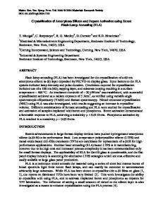
Conductance measurements The samples are crystallized by annealing under vacuum at different temperatures, in the range 550-650 TC. The SPC of the amorphous layers was studied by in-situ monitoring the film conductance. The experimental set-up consists of two molybdenum electrodes placed on the sample surface.Under these conditions, variations of the layer conductance with the annealing time can be measured. Figure 1 shows the typical behaviour of the normalized conductance variation. Ca co
1.0-
1.0-
0.8
z 0.8-
w 0.6-
00 0.6-
V 0.4-
o0.4-
0.
0.2-:
I0~
I
Data Loading...